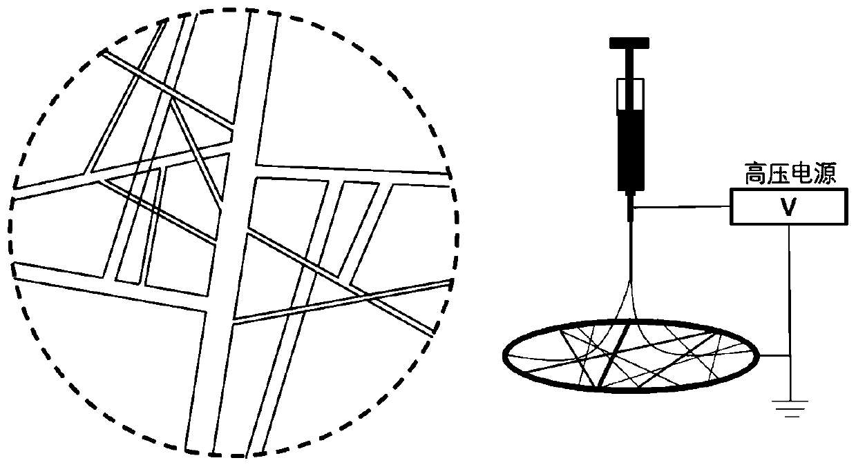
Infrared regulation and control bionic laminated device
A stacking and device technology, applied in the field of infrared control, can solve the problems of the same color and different spectrum, the lack of natural leaf tissue structure and composition characteristics, and the difference in the real characteristics of leaves, so as to achieve the enhancement of hyperspectral bionic characteristics and improve the infrared transmission performance. Effect
- Summary
- Abstract
- Description
- Claims
- Application Information
AI Technical Summary
Problems solved by technology
Method used
Image
Examples
Embodiment 1
[0023] An infrared control bionic laminated device, the preparation process is as follows:
[0024] Step 1. Preparation of the top biomimetic electrode:
[0025] 1.1 Select polyvinylpyrrolidone as the electrode structure template, dissolve polyvinylpyrrolidone (Mr=1300000) in absolute ethanol, and prepare a precursor solution with uniform viscosity; transfer the prepared precursor solution to the spinning tube, and use electrospinning The electrode template was obtained by the method, the spinneret with a diameter of 0.25mm, the airflow pressure of 0.26MPa, the air duct width of 0.4mm, the air duct angle of 60°, and the receiving distance of 20mm were selected, and the spinning voltage (8kV, 10kV, 12kV) was adjusted to change the polymer Whip during the fiber forming process to obtain nanofibers with different diameters, and collect the polymer fibers into a copper frame vessel, so as to realize the preparation of nanofibers with diameters of 600nm, 1300nm and 2400nm in the sa...
Embodiment 2
[0035] An infrared control bionic laminated device, the preparation process is as follows:
[0036] Step 1. Preparation of the top-layer biomimetic electrode: select metal gold as the electrode material, first prepare a gold film with a thickness of 80 μm on the PET substrate by magnetron sputtering, and then spin-coat a uniform layer of gold film on the surface of the gold film to be etched. Photoresist, after soft baking, a layer of photoresist film can be formed on the surface, and then through the process of ultraviolet exposure, development, shaping and hardening, the pattern with vein structure on the mask plate can be accurately transferred to the photolithography of the metal surface Finally, use inductively coupled plasma etching method to etch and remove the part not covered by the photoresist on the gold film. After removing the photoresist, the top biomimetic electrode with leaf vein structure is obtained;
[0037] Step 2. Preparation of the electrovariable infrare...
PUM
| Property | Measurement | Unit |
|---|---|---|
| diameter | aaaaa | aaaaa |
| diameter | aaaaa | aaaaa |
| diameter | aaaaa | aaaaa |
Abstract
Description
Claims
Application Information


