Horizontal nanochannel array, micro-nanofluidic chip and manufacturing method thereof
A manufacturing method and nanochannel technology, applied in nanotechnology, chemical instruments and methods, laboratory equipment, etc., can solve problems such as inability to mass produce, complex fabrication methods of micro-nano flow channel chips, and incompatibility between technology and integrated circuit technology , to achieve the effect of simple process
- Summary
- Abstract
- Description
- Claims
- Application Information
AI Technical Summary
Problems solved by technology
Method used
Image

Examples
Embodiment 1
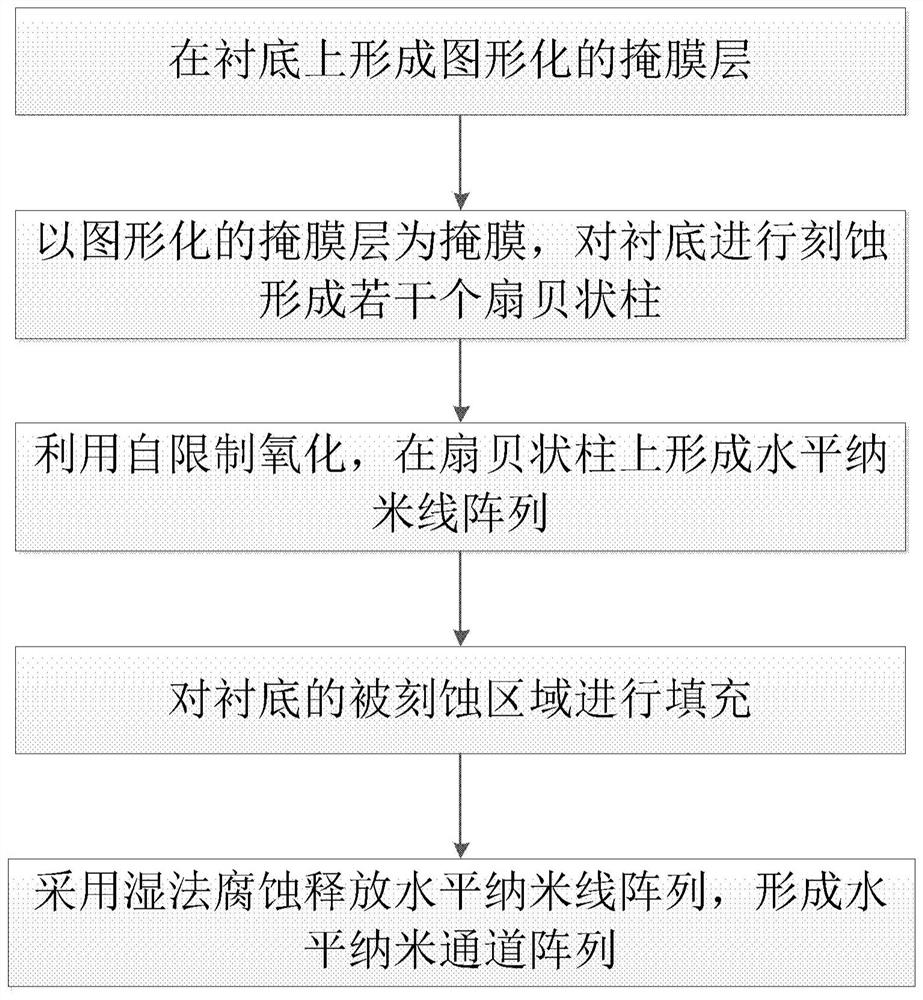
[0034] In the first exemplary embodiment of the present invention, a method of manufacturing a horizontal nanochannel array, such as figure 1 As shown, including the following steps:
[0035] Step 1: Form a graphical mask layer 2 on the substrate 1;
[0036] Step 2: The substrate 1 is etched to form a plurality of scallop columns 3;
[0037] Step 3: Using self-limiting oxidation, a horizontal nanowire array 4 is formed on the scallop column 3;
[0038] Step 4: Fill the etching region of the substrate 1;
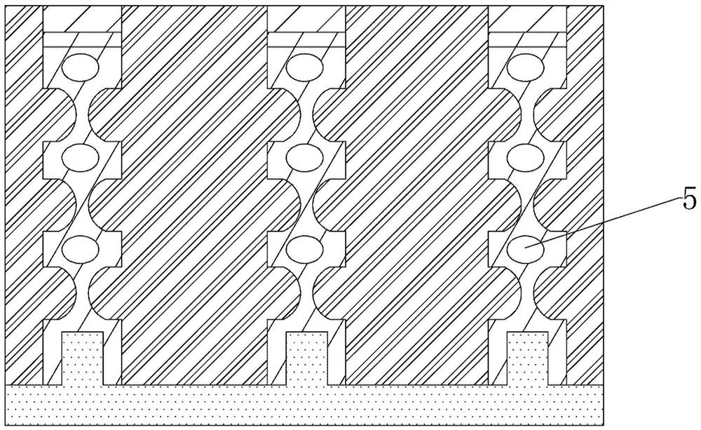
[0039] Step 5: Release the horizontal nano-channel array 5 by wet corrosion release horizontal nano-channel array 5.
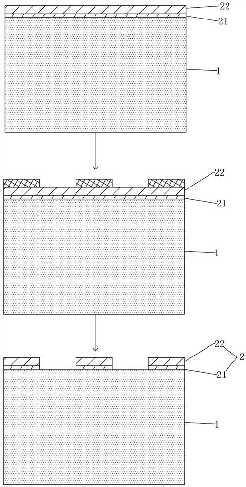
[0040] In an embodiment of the invention, if image 3 As shown, step 1 specifically includes the following steps:
[0041] Sub-step 111: Form a mask layer on the substrate 1;
[0042] More specifically, the mask layer is from the lower to upper, and the silicon oxide layer 21 and the silicon nitride layer 22 may be a chemical vapor deposition method or a thermal o...
Embodiment 2
[0071] In a second exemplary embodiment of the present invention, a method of fabricating a horizontal nanochannel array is provided, wherein the embodiment is different from that of the first embodiment in that the substrate 1 is etched in the step 2. The specific step of several sectors 3 is, etching the substrate 1 is etched to form a plurality of scallop column 3 using the Bosch process.
[0072] Among them, the Bosch process is specifically C. 4 Fly 8 SF 6 The gas is repeatedly deposited and etched by the substrate 1, forming a plurality of scallop column 3;
[0073] Among them, the number of etching cycles is the same as the number of nanowires in the horizontal nanowire array 4.
Embodiment 3
[0076] In a third exemplary embodiment of the present invention, a method of fabricating a horizontal nanochannel array is provided, wherein the embodiment is different from that of Example 1 is: Figure 4 As shown, step 1 includes the following steps:
[0077] Sub-step 121: Sequentially form the silicon oxide layer 21 and silicon layer 23 on the substrate 1;
[0078] Sub-step 122: Anisotropic etching of the silicon layer 23 to form a silicon step;
[0079] Sub-step 123: A silicon nitride layer 22 is formed on the silicon oxide layer 21 having a silicon step;
[0080] Sub-step 124: Adding from self-alignment etching to form a silicon nitride side wall;
[0081] Sub-step 125: Sequentially remove the silicon step and the bare silicon oxide layer 21 by wet corrosion, forming a graphical mask layer 2;
[0082] Wherein, the silicon layer 23 is a polysilicon layer or an amorphous silicon layer;
[0083] In an embodiment of the present invention, the silicon step is a smooth and steepmost...
PUM
| Property | Measurement | Unit |
|---|---|---|
| width | aaaaa | aaaaa |
Abstract
Description
Claims
Application Information
 - R&D
- Intellectual Property
- Life Sciences
- Materials
- Tech Scout
- Unparalleled Data Quality
- Higher Quality Content
- 60% Fewer Hallucinations
Browse by: Latest US Patents, China's latest patents, Technical Efficacy Thesaurus, Application Domain, Technology Topic, Popular Technical Reports.
© 2025 PatSnap. All rights reserved.Legal|Privacy policy|Modern Slavery Act Transparency Statement|Sitemap|About US| Contact US: help@patsnap.com