Atomic layer deposition apparatus and 3D storage device

A technology of atomic layer deposition and equipment, which is applied in the manufacture of electrical solid devices, semiconductor devices, semiconductor/solid devices, etc., can solve problems such as device failure, improve adhesion, increase yield and reliability, and have consistent crystal orientation Effect

Active Publication Date: 2020-08-25
YANGTZE MEMORY TECH CO LTD
View PDF5 Cites 0 Cited by
  • Summary
  • Abstract
  • Description
  • Claims
  • Application Information

AI Technical Summary

Problems solved by technology

In the step of filling the metal material, the metal material is generated by reducing metal fluoride, and the generated fluorine can diffuse into the interlayer insulating layer through the adhesive film, so that the gate conductors at different levels are interconnected, or the channel pillars are interconnected. even, may still result in device failure

Method used


Image

  • Atomic layer deposition apparatus and 3D storage device
  • Atomic layer deposition apparatus and 3D storage device
  • Atomic layer deposition apparatus and 3D storage device

Examples


Embodiment Construction

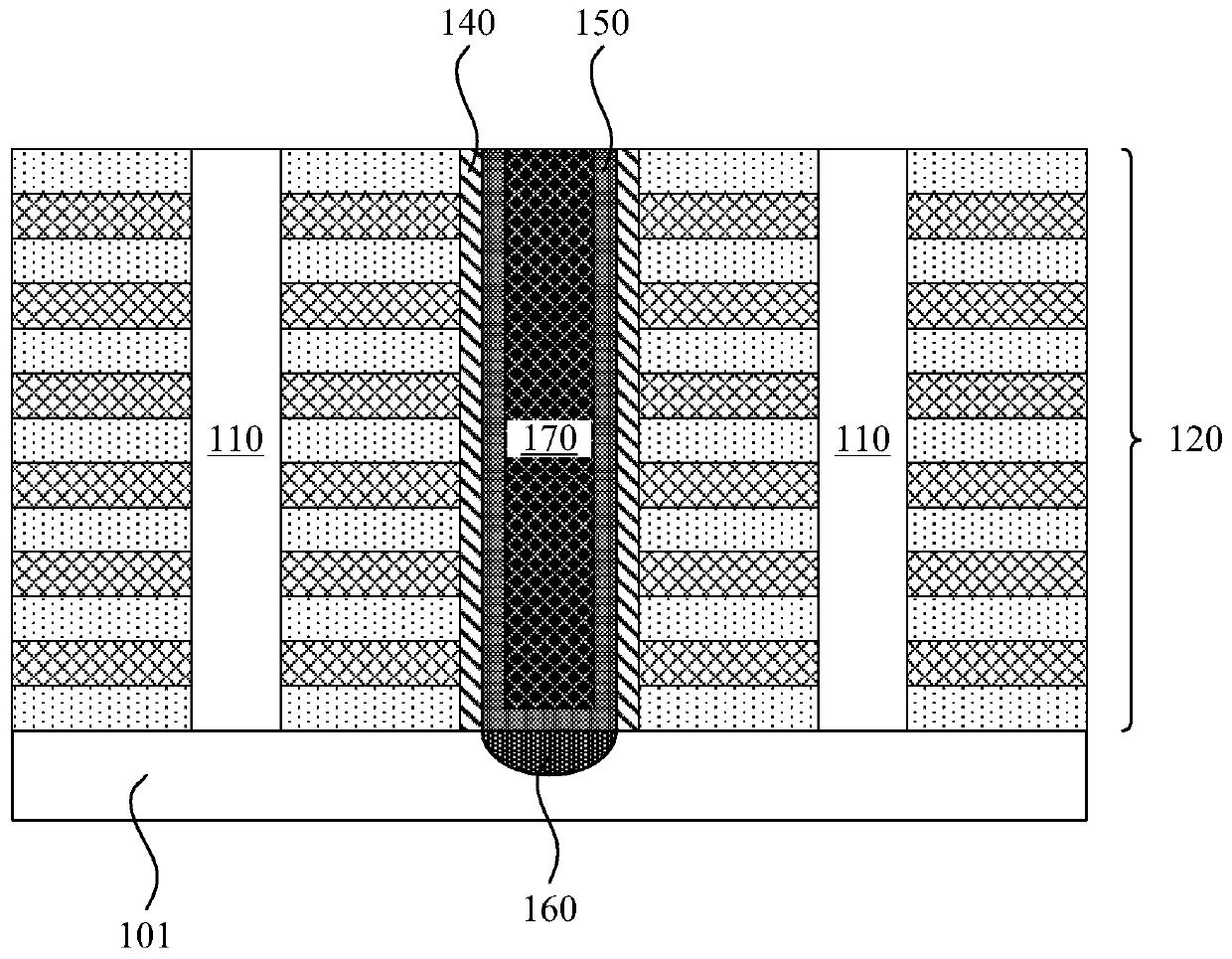
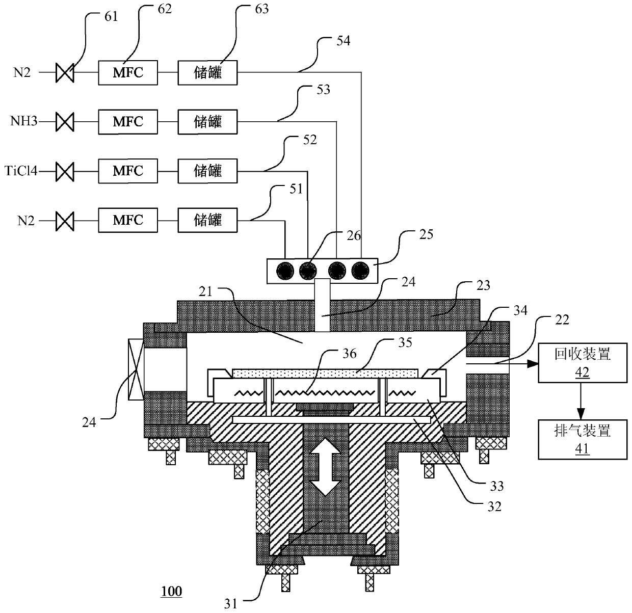
[0025] Hereinafter, various embodiments of the present invention will be described in more detail with reference to the accompanying drawings. In the various drawings, the same elements are represented by the same or similar reference numerals. For the sake of clarity, the various parts in the drawings are not drawn to scale.

[0026] The present invention will be described in more detail below with reference to the accompanying drawings. In the various drawings, the same elements are represented by similar reference numerals. For the sake of clarity, the various parts in the drawings are not drawn to scale. In addition, some well-known parts may not be shown. For the sake of brevity, the semiconductor structure obtained after several steps can be described in one figure.

[0027] It should be understood that when describing the structure of the device, when a layer or region is referred to as being "on" or "above" another layer or another region, it can mean directly on the ot...


PUM


Abstract

The invention discloses an atomic layer deposition apparatus and a 3D storage device. The atomic layer deposition apparatus comprises an air inlet pipeline used for receiving at least two kinds of reactant gas and inert gas, a reaction chamber connected with the air inlet pipeline, a base located in the reaction chamber and used for bearing a silicon wafer and heating the silicon wafer, and an exhaust channel connected with the reaction chamber, the atomic layer deposition apparatus further comprises an adjustable control board located in the reaction chamber and used for blocking the reactantgas from arriving at the surface of the silicon wafer, according to the atomic layer deposition apparatus, the adjustable control board controls the reactant gas participating in the silicon wafer surface reaction, an adhesive film can carry out layered growth, the adhesive film with the consistent crystal orientation and the crystal boundary superficial area reduced is obtained, and the blockingcapacity of the adhesive film is improved.

Description

Technical field [0001] The invention relates to the technical field of semiconductor manufacturing, in particular to an atomic layer deposition equipment and a 3D storage device. Background technique [0002] The improvement of the storage density of the storage device is closely related to the progress of the semiconductor manufacturing process. As the feature size of the semiconductor manufacturing process becomes smaller and smaller, the storage density of the memory device becomes higher and higher. In order to further increase the storage density, storage devices with three-dimensional structures (ie, 3D storage devices) have been developed. The 3D memory device includes a plurality of memory cells stacked in a vertical direction, and the integration degree can be doubled on a wafer of unit area, and the cost can be reduced. [0003] In the manufacturing process of 3D memory devices, for example, an etching method is used to form a cavity in the interlayer insulating layer, ...

Claims


Application Information

Patent Timeline
Patent Type & Authority Applications(China)
IPC IPC(8): C23C16/455H01L21/768H01L27/11521H01L27/11551H01L27/11568H01L27/11578
CPCC23C16/45544C23C16/45589H01L21/76841H10B41/20H10B43/30H10B43/20H10B41/30
Inventor 李远博宋锐李远孙祥烈
Owner YANGTZE MEMORY TECH CO LTD
Why Eureka
Try Eureka