Manufacturing method of high-flatness multilayer circuit board

A technology of multilayer circuit board and manufacturing method, which is applied in the direction of multilayer circuit manufacturing, printed circuit manufacturing, printed circuit, etc., can solve the problems of uneven surface of multilayer circuit board, large amount of line erosion, etc., and prevent the problem of uneven surface , the effect of reliable conductivity

Pending Publication Date: 2020-08-25
DIGITAL PRINTED CIRCUIT BOARD CO LTD
View PDF3 Cites 2 Cited by
  • Summary
  • Abstract
  • Description
  • Claims
  • Application Information

AI Technical Summary

Problems solved by technology

[0005] In view of the above problems, the present invention provides a method for manufacturing a multilayer circuit board with high flatness, which can solve the problems of uneven surface and excessive line erosion of the multilayer circuit board produced in the prior art

Method used


Image

  • Manufacturing method of high-flatness multilayer circuit board
  • Manufacturing method of high-flatness multilayer circuit board
  • Manufacturing method of high-flatness multilayer circuit board

Examples


Embodiment Construction

[0038] The present invention will be further described in detail below with reference to the examples and drawings, but the implementation of the present invention is not limited thereto.

[0039] refer to Figure 3-5 Shown:

[0040] A method for manufacturing a multilayer circuit board with high flatness, comprising the following steps:

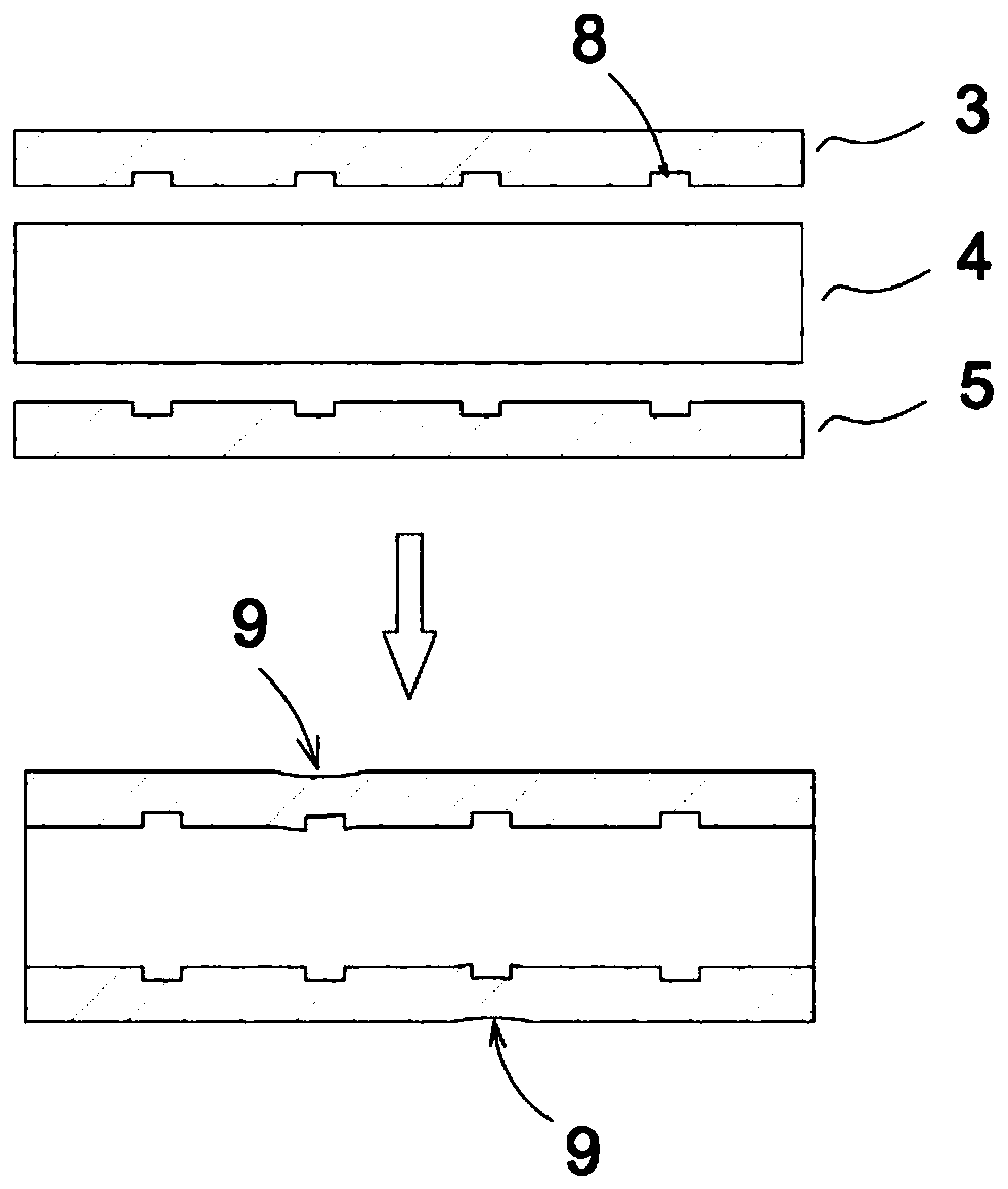
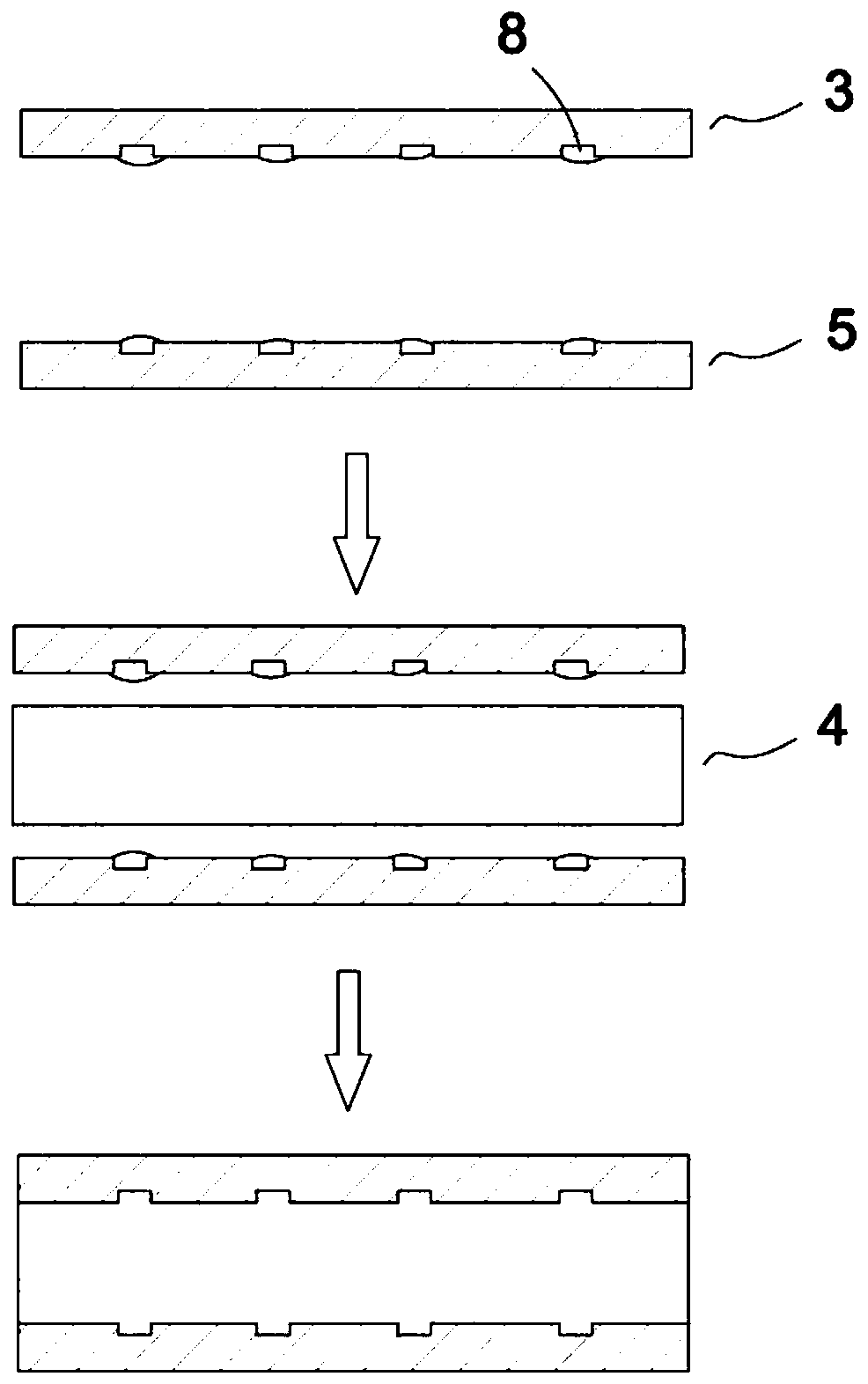
[0041] S1 material preparation: prepare the upper layer board 1, the first prepreg board 2, the first copper substrate 3, the second prepreg board 4, the second copper substrate 5, the third prepreg board 6, and the lower board 7;

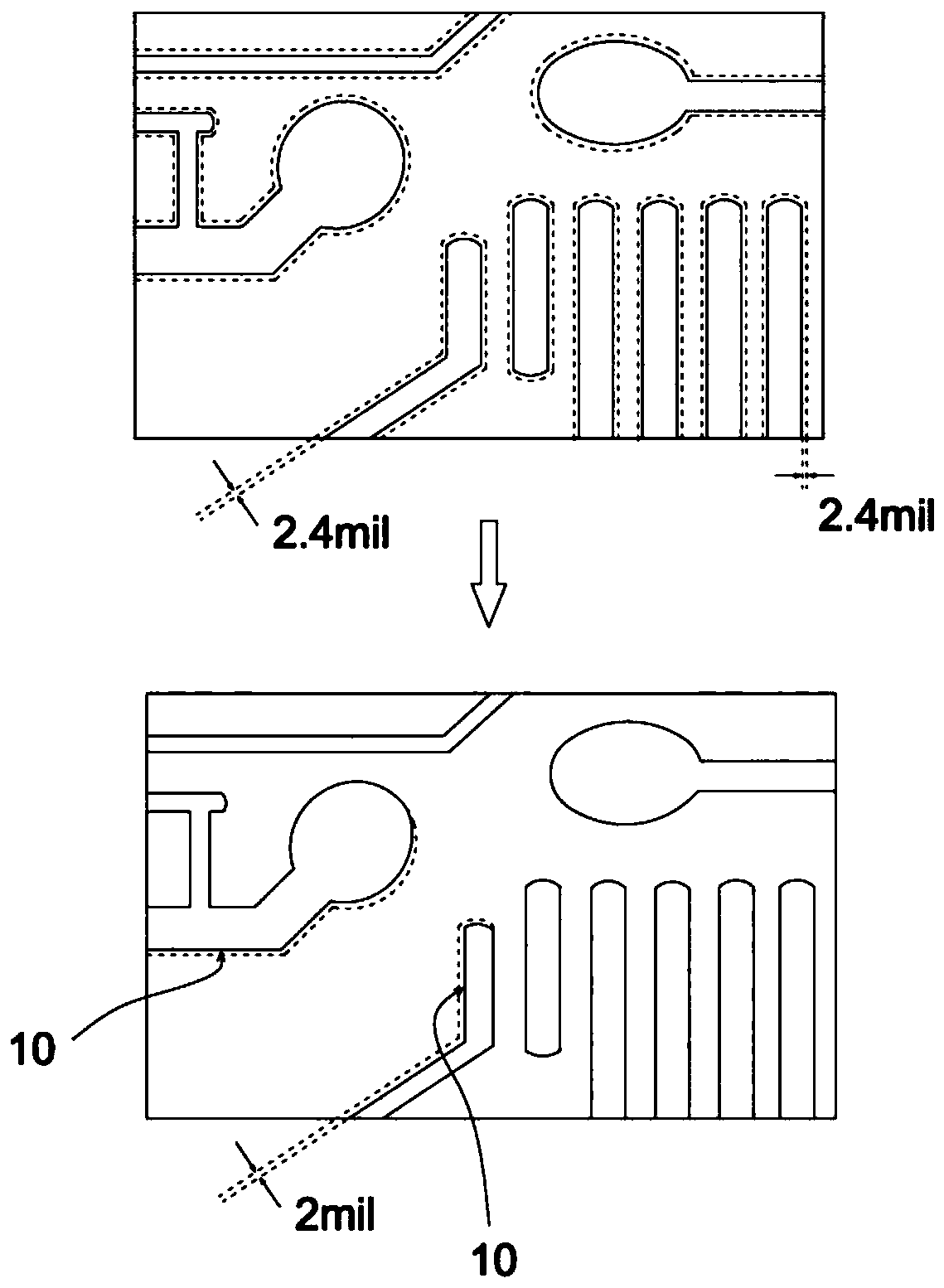
[0042] S2 First copper substrate treatment: apply film, develop, expose, and etch the lower end surface of the first copper substrate 3, and obtain the hollowed-out first inner layer circuit after removing the film, and make target holes on the first copper substrate 3 for target shooting After the holes are made, target holes are made on the first copper substrate 3. Since the first copper substrate 3, the sec...


PUM


Abstract

The invention provides a manufacturing method of a high-flatness multilayer circuit board. The manufacturing method comprises the following steps of material preparation, first copper substrate processing, second copper substrate processing, primary resin joint filling, primary press fit, inner layer board processing, secondary resin joint filling, secondary press fit, drilling, copper plating, film drying, etching, tin plating, solder masking, secondary solder masking, character forming and pattern fishing. The problems of uneven surface and overlarge line etching amount of the multilayer circuit board manufactured in the prior art can be solved.

Description

technical field [0001] The invention relates to the technical field of circuit board processing, in particular to a method for manufacturing a multilayer circuit board with high flatness. Background technique [0002] A circuit board, also known as a printed circuit board, is the provider of electrical connections for electronic components. Its development has a history of more than 100 years, and its design is mainly layout design. The main advantage of using circuit boards is that it greatly reduces wiring and assembly errors, and improves the automation level and production labor rate. According to the number of layers of circuit boards, printed circuit boards can be divided into single-sided boards, double-sided boards, four-layer boards, six-layer boards and other multi-layer circuit boards. [0003] For multi-layer circuit boards, some of its processing processes are as follows: figure 1 As shown, usually the first copper substrate 3, the second prepreg 4, and the se...

Claims


Application Information

Patent Timeline
Patent Type & Authority Applications(China)
IPC IPC(8): H05K3/06H05K3/00H05K3/46H05K3/28
CPCH05K3/06H05K3/0047H05K3/4611H05K3/282H05K3/0085H05K3/0044H05K3/00
Inventor 王锋
Owner DIGITAL PRINTED CIRCUIT BOARD CO LTD
Why Eureka
Try Eureka