Abrasive material for large-diameter silicon wafer and production method thereof

A technology for abrasive materials and production methods, applied in chemical instruments and methods, other chemical processes, electrical components, etc., can solve the problem that the ratio of various raw materials of abrasive materials is not easy to grasp, and achieve processing stability, increased effect, particle size, etc. selective enhancement

Inactive Publication Date: 2020-09-01
无锡成旸科技股份有限公司
View PDF13 Cites 0 Cited by
  • Summary
  • Abstract
  • Description
  • Claims
  • Application Information

AI Technical Summary

Problems solved by technology

[0004] Aiming at the deficiencies of the prior art, the present invention provides an abrasive material for large-diameter silicon wafers and a production method thereof, which effectively optimizes the advantages of the proportion separation of the abrasive material and solves the problem of various raw material proportions of the abrasive material in the separation process. Choose questions that are not easy to grasp

Method used


Image

  • Abrasive material for large-diameter silicon wafer and production method thereof
  • Abrasive material for large-diameter silicon wafer and production method thereof
  • Abrasive material for large-diameter silicon wafer and production method thereof

Examples


Embodiment Construction

[0029] The technical solutions in the embodiments of the present invention will be clearly and completely described below in conjunction with the embodiments of the present invention. Obviously, the described embodiments are only a part of the embodiments of the present invention, rather than all the embodiments. Based on the embodiments of the present invention, all other embodiments obtained by those of ordinary skill in the art without creative work shall fall within the protection scope of the present invention.

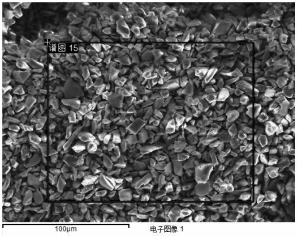
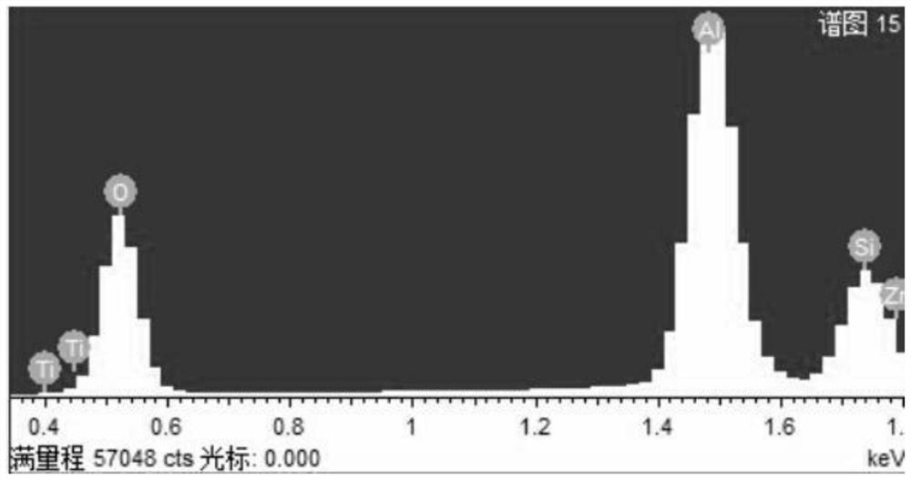
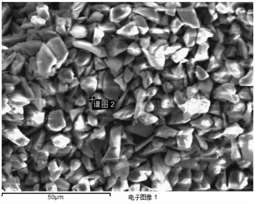
[0030] An abrasive material for large-diameter silicon wafers and a production method thereof, comprising the following raw materials in parts by mass: 45% zirconium silicate ZrSiO4, 55% alumina Al2O3, a small amount of catalyst and a small amount of binding agent, silicic acid The mass of zirconia in zirconium ranges from 25% to 35%.

[0031] First, the selected zirconium silicate and the selected alumina are introduced into the mixing bin according to the mass ratio...


PUM

PropertyMeasurementUnit
densityaaaaaaaaaa

Abstract

The invention relates to the technical field of silicon wafer abrasive material production methods. The invention further discloses an abrasive material for a large-diameter silicon wafer and a production method of the abrasive material. The abrasive material comprises the following raw materials in parts by mass: 45% of zirconium silicate ZrSiO4, 55% of aluminum oxide Al2O3, a small amount of a catalyst and a small amount of a binding agent. Firstly, zirconium silicate and aluminum oxide are guided into a mixing bin according to the mass ratio to be evenly mixed and stirred, the mixture is guided into a rotary kiln to be sintered after being evenly stirred, a catalyst and a binding agent are added, and after sintering is completed, a semi-finished product is guided into a jet mill crusherto be subjected to particle crushing. Compared with other composite grinding materials, the difference between the production method adopted by the invention and the production methods of the other composite grinding materials is that two materials are used for calcining to obtain particles with relatively close physical properties and chemical properties, and the ratio of the two materials withdifferent properties can be kept unchanged, so that the uniformity of the product in processing and use is thoroughly changed, and the use effect is greatly improved due to the characteristics of thematerials.

Description

Technical field [0001] The invention relates to the technical field of production methods for silicon wafer abrasive materials, in particular to an abrasive material for large-diameter silicon wafers and a production method thereof. Background technique [0002] There are two existing high-end abrasive materials, one is high-purity alumina abrasive material and the other is composite abrasive material. The high-purity alumina abrasive material has the characteristics of controllable particle size and high grinding efficiency. The material has the characteristics of high surface quality after grinding and not easy to cause scratches. The various raw materials of composite abrasive materials are different in physical properties, so the consistency cannot be guaranteed during processing and use. The biggest impact is that the ratio of various raw materials is not easy to grasp in the sorting, which causes the use effect to decrease. The inventor designed an abrasive material for la...

Claims


Application Information

Patent Timeline
Patent Type & Authority Applications(China)
IPC IPC(8): C09K3/14H01L21/304
CPCC09K3/1418C09K3/1436H01L21/304
Inventor 马豪军虞向荣
Owner 无锡成旸科技股份有限公司
Why Eureka
Try Eureka