Supercharge Your Innovation With Domain-Expert AI Agents!

Three-terminal optoelectronic components with improved matching of electric field and photocurrent density

A terminal, avalanche photoelectric technology, applied in electrical components, electrical solid devices, circuits, etc., can solve problems such as loss

Active Publication Date: 2022-04-26
HEWLETT-PACKARD ENTERPRISE DEV LP
View PDF2 Cites 0 Cited by
  • Summary
  • Abstract
  • Description
  • Claims
  • Application Information

AI Technical Summary

Problems solved by technology

Second, some of the source light may be lost in waveguides and other optics in the circuit

Method used


Image

  • Three-terminal optoelectronic components with improved matching of electric field and photocurrent density
  • Three-terminal optoelectronic components with improved matching of electric field and photocurrent density
  • Three-terminal optoelectronic components with improved matching of electric field and photocurrent density

Examples


Embodiment Construction

[0022] The description of the various advantageous examples has been presented for purposes of illustration and is not intended to be exhaustive or limited to the examples in the form disclosed. Many modifications and changes will be apparent to those of ordinary skill in the art. Additionally, different advantageous examples may offer different advantages over other advantageous examples. The selected example or examples were chosen and described in order to best explain the principles of these examples, the practical application, and to enable others of ordinary skill in the art to understand the disclosure with various modifications as are suited to the intended use. kind of example.

[0023] Before the present disclosure is described in detail, it is to be understood that unless otherwise indicated, this disclosure is not limited to particular processes or articles of manufacture, whether described or not. It should also be understood that the terminology used herein is ...


PUM


Abstract

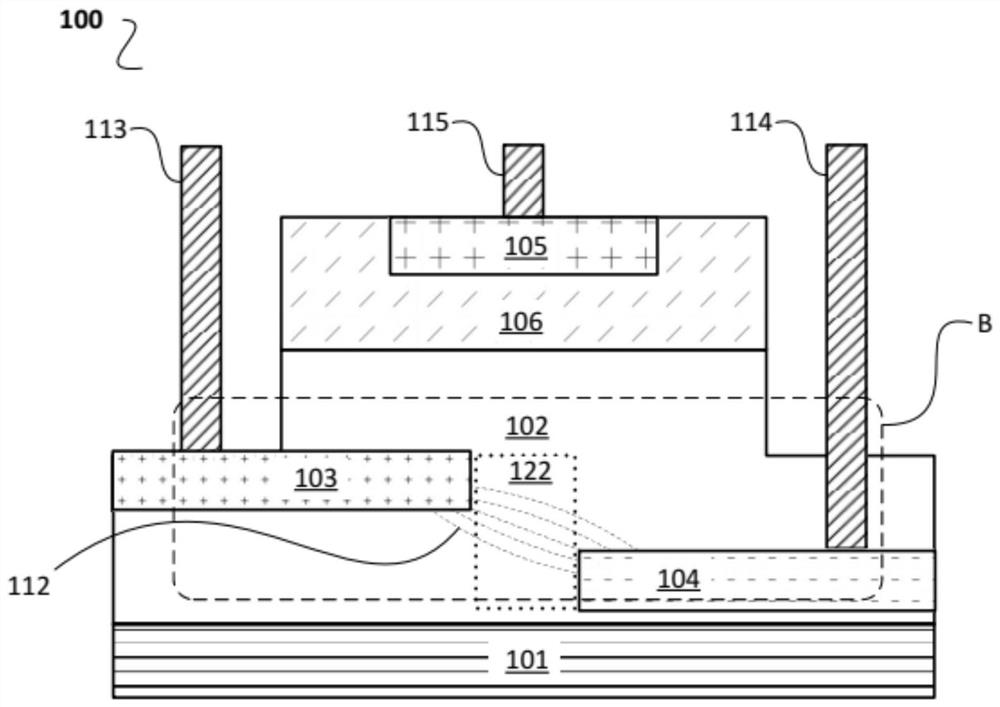
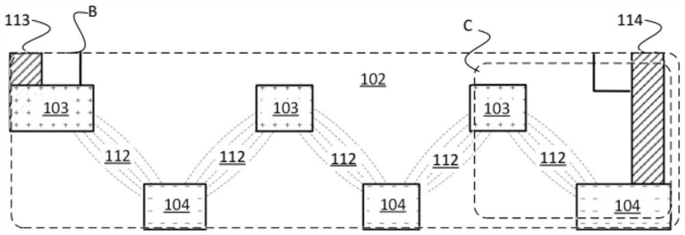
A three-terminal avalanche photodiode provides a first controllable voltage drop across a light absorption region and a second independently controllable voltage drop across a photocurrent amplification region. The composition of the absorption region and the amplification region can be optimized independently of each other. In the enlarged region, the p-doped structure and the n-doped structure are offset from each other in both the horizontal direction and the vertical direction. Applying a voltage directly across the controlled region of the photocurrent path increases the avalanche gain by shaping the electric field to overlap the photocurrent density. The resulting high-gain, low-bias avalanche photodiodes can be fabricated in integrated optical circuits using commercial CMOS processes, operated from power supplies commonly used in mature computer architectures, and used for optical interconnects, light sensing, and other applications.

Description

technical field [0001] The present disclosure generally relates to avalanche photodiodes, computing devices, and methods for fabricating optoelectronic components. Background technique [0002] In the field of optoelectronics, integrated optical circuits or subassemblies can be designed to replace their electronic counterparts in computing devices, signal processing devices, and other devices. The cost of fabricating large-scale optical circuits, especially silicon photonic devices, has decreased significantly in recent years. However, all-optical devices may still not be practical for some applications. In some devices, high-speed and / or broadband optics can be strategically combined with low-power or low-cost electronics. Photodetectors, which convert optical signals to electrical signals, play a key role at the interface between optical and electronic components. [0003] Optical signal levels in integrated optical circuits can be very low. First, light sources are ty...

Claims


Application Information

Patent Timeline
IPC IPC(8): H01L31/107H01L31/0352H01L31/18
CPCH01L31/107H01L31/1075H01L31/035272H01L31/1804H01L31/022408H01L25/167Y02P70/50H01L31/1129H01L31/02027
Inventor 曾小鸽黄志宏梁迪
Owner HEWLETT-PACKARD ENTERPRISE DEV LP
Features
  • R&D
  • Intellectual Property
  • Life Sciences
  • Materials
  • Tech Scout
  • Unparalleled Data Quality
  • Higher Quality Content
  • 60% Fewer Hallucinations
Learn More