Power amplifier chip biasing circuit based on GaAs HBT process

A bias circuit and power amplifier chip technology, applied in the direction of adjusting electrical variables, control/regulation systems, instruments, etc., can solve the problems of unsuitable power tubes, limit circuit universality, increase area cost, etc., and achieve easy on-chip integration, Good promotion value, simple structure effect

Active Publication Date: 2020-09-15
SOUTH CHINA UNIV OF TECH
View PDF5 Cites 2 Cited by
  • Summary
  • Abstract
  • Description
  • Claims
  • Application Information

AI Technical Summary

Problems solved by technology

In order to suppress the problems of power amplifier gain change and linearity drop caused by temperature changes, an off-chip voltage regulation structure or an on-chip temperature sensing structure can be used, but such methods increase power consumption and increase area costs, so A more effective way is to use the on-chip temperature drift suppression bias circuit to provide a bias voltage or bias current that is not affected by temperature as much as possible.
At present, a variety of on-chip circuit structures have been proposed. There is a circuit that uses Zener diodes to automatically compensate temperature drift. Diode clamping is not suitable for large-area power tubes; there are high-order temperature-compensated bandgap reference circuits that use diodes instead of BJT tubes, and there are bias circuits that realize temperature detection and compensation amplification through a structure similar to differential voltage. This kind of circuit improves the accuracy and reduces the temperature coefficient at the same time, but it also faces the challenge of mobile communication equipment with higher and higher integration. The consumption of area and power consumption limits the universality of this kind of circuit; The circuit combining the current converter and the PTAT current realizes the temperature-compensated dB linear gain control, and also reduces the area, but the output voltage level is single, and it cannot provide voltage compensation with multi-layer temperature coefficients to prevent excessive bias voltage. breakdown

Method used


Image

  • Power amplifier chip biasing circuit based on GaAs HBT process
  • Power amplifier chip biasing circuit based on GaAs HBT process
  • Power amplifier chip biasing circuit based on GaAs HBT process

Examples


Embodiment 1

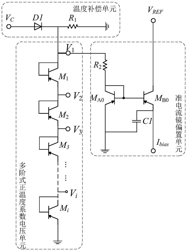
[0024] Embodiment 1, the current mirror includes a capacitor C1, a first input side HBT transistor M A0 and the first output side HBT tube M B0 . The first input side HBT tube M A0 As the input side, the first output side HBT tube M B0 as the output side. HBT tube M on the first input side A0 After the base and the collector are short-circuited, they are connected to the second positive temperature coefficient resistor R2, and the emitter is grounded. HBT tube M on the first output side B0 The base is connected to the first input side HBT tube M A0 The base, collector external reference voltage V REF , the emitter is used for external output bias current I bias . The capacitor C1 is connected to the first output side HBT tube M B0 between emitter and ground.

Embodiment 2

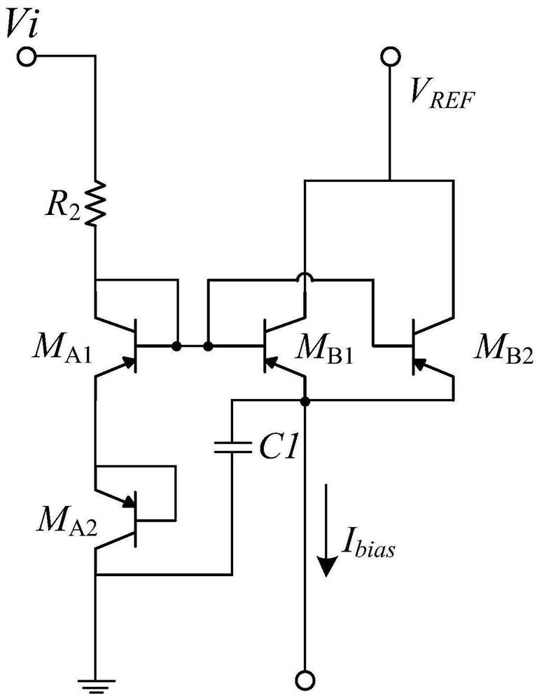
[0025] Embodiment two, such as figure 2 As shown, the current mirror includes capacitor C1, the second input side HBT tube M A1 , the third input side HBT tube M A2 , the second output side HBT tube M B1 and the third output side HBT tube M B2 . The second input side HBT tube M A1 and the third input side HBT tube M A2 Composing the input side, the second output side HBT tube MB1 and the third output side HBT tube M B2 form the output side. The second input side HBT tube M A1 The base and the collector are short-circuited and connected to the second positive temperature coefficient resistor R2, and the emitter is connected to the third input side HBT tube M A2 the emitter. The third input side HBT tube M A2 The base and emitter are shorted and the collector is grounded. The second output side HBT tube M B1 and the third output side HBT tube M B2 Connect in parallel, connect the second input side HBT tube M after the base is common A1 The base and the collector a...


PUM


Abstract

The invention discloses a power amplifier chip biasing circuit based on a GaAs HBT process, and relates to a new generation information technology, thereby solving a problem that in the prior art, a temperature compensation means has negative effects on size, power and the like. A diode and a first resistor are used for obtaining temperature induction resistance; meanwhile, a plurality of HBT tubes are connected in series to replace traditional resistors, a bias voltage is led out from each HBT tube, and multi-order positive temperature coefficient voltage output is achieved. Furthermore, thevoltage is converted through a current mirror and a positive temperature coefficient second resistor, and a bias current for temperature drift suppression is provided for the power amplifier chip. Andthe requirements of mobile equipment on high integration level, high power output, high stability and low cost are effectively met. Therefore, strict requirements of the power amplifier chip of the mobile equipment in the aspects of size, power consumption, long-term sustainable work and the like can be met with very low complexity and relatively high reliability in the aspect of implementation,and the power amplifier chip biasing circuit has a good popularization value.

Description

technical field [0001] The invention relates to radio frequency chip technology, in particular to a power amplifier chip bias circuit based on GaAs HBT technology. Background technique [0002] The gradual arrival of the 5G era has brought more serious challenges to the RF front-end chips of mobile terminal equipment, especially the power amplifier chip, as one of the most important RF modules in the communication system, located at the end of the transmitter, its performance directly Affect the transmission distance and transmission quality of the signal. However, no matter what process is used to design the power amplifier chip, its output performance is seriously affected by the external temperature and self-heating effect. On the outside, in cold regions with extreme living conditions, the temperature can reach as low as -20°C; on the inside, due to the influence of large output power, high power density and high operating frequency band, the thermal coupling between th...

Claims


Application Information

Patent Timeline
Patent Type & Authority Applications(China)
IPC IPC(8): G05F1/567
CPCG05F1/567
Inventor 李斌马渊博吴朝晖
Owner SOUTH CHINA UNIV OF TECH
Why Eureka
Try Eureka