Manufacturing method of double-sided photoelectric substrate with interconnected high-density through holes

A manufacturing method and high-density technology, applied in the direction of final product manufacturing, sustainable manufacturing/processing, semiconductor/solid-state device manufacturing, etc., can solve the problems of large precision error, low processing efficiency, and difficult Pt film patterning, etc. achieve the effect of effective combination

Active Publication Date: 2020-09-18
XIAN MICROELECTRONICS TECH INST
View PDF4 Cites 3 Cited by
  • Summary
  • Abstract
  • Description
  • Claims
  • Application Information

AI Technical Summary

Problems solved by technology

[0003] The purpose of the present invention is to overcome the shortcoming of above-mentioned prior art, provide a kind of manufacture method of the double-sided optoelectronic substrate of high-density through-hole interconnection; , the process is complicated, the processing efficiency is low, the Pt film layer is difficult to pattern, and the accuracy error is large, etc.

Method used


Image

  • Manufacturing method of double-sided photoelectric substrate with interconnected high-density through holes
  • Manufacturing method of double-sided photoelectric substrate with interconnected high-density through holes
  • Manufacturing method of double-sided photoelectric substrate with interconnected high-density through holes

Examples


Embodiment Construction

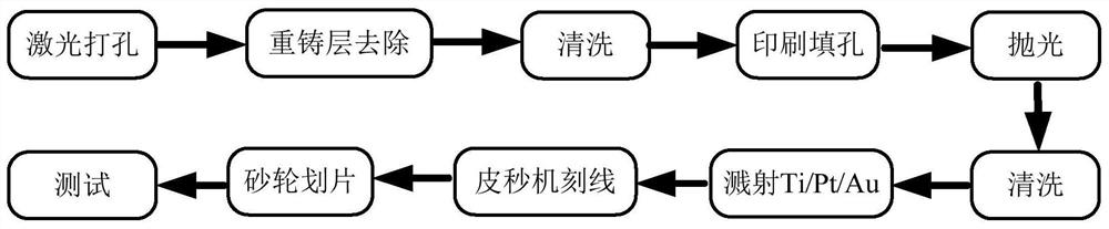
[0044] The present invention is described in further detail below in conjunction with accompanying drawing:

[0045] In the description of the present invention, it should be noted that the terms "center", "upper", "lower", "left", "right", "vertical", "horizontal", "inner", "outer" etc. The indicated orientation or positional relationship is based on the orientation or positional relationship shown in the drawings, and is only for the convenience of describing the present invention and simplifying the description, rather than indicating or implying that the referred device or element must have a specific orientation, or in a specific orientation. construction and operation, and therefore cannot be construed as limiting the present invention; the terms "first", "second", and "third" are used for descriptive purposes only, and cannot be construed as indicating or implying relative importance; in addition, unless otherwise Clearly stipulated and limited, the terms "installation"...


PUM

PropertyMeasurementUnit
surface roughnessaaaaaaaaaa
thicknessaaaaaaaaaa
surface roughnessaaaaaaaaaa

Abstract

The invention discloses a manufacturing method of a double-sided photoelectric substrate with interconnected high-density through holes. According to the method, the double-sided interconnected photoelectric ceramic substrate with the high-density micro-through holes is manufactured on the basis of the processes of manufacturing the micro-through holes in the ceramic substrate by a laser processing technology, filling the auxiliary through holes, flattening the surface, sputtering a film layer, manufacturing wiring lines and the like. The method is based on a fine processing technology of AlNceramic by laser. The manufacturing technology of the high-density micro-through-hole interconnection photoelectric device is studied, through the high-density micro-through-hole double-face interconnection technology, the double sides of the substrate are connected via the through holes, Au is filled in the through holes, and the problems that the back face of a photoelectric module device circuit needs to have corresponding functions and is connected with a front face graph and reliability is poor are solved. A metal film layer is prepared on the basis of a magnetron sputtering technology, the high-density micro-through-hole interconnection photoelectric device manufacturing technology is realized, a patterning process technology is carried out through a metallization layer, and a thickfilm hole filling process and a thin film patterning process are effectively combined.

Description

【Technical field】 [0001] The invention belongs to the technical field of photoelectric substrate manufacturing, and in particular relates to a method for manufacturing a double-sided photoelectric substrate with high-density through-hole interconnection. 【Background technique】 [0002] With the gradual development of electronic packaging technology towards miniaturization, high density, multi-function and high reliability, higher requirements are put forward for devices. As the core device of microelectronics manufacturing, optoelectronic substrate must be assembled with high reliability in accordance with the corresponding development plan. In order to increase the assembly density of optoelectronic substrates, high-precision double-sided interconnection of devices must be realized. At present, laser processing technology has been widely used in the processing of aviation and spacecraft components, such as laser drilling technology and etching technology. Because AlN cera...

Claims


Application Information

Patent Timeline
Patent Type & Authority Applications(China)
IPC IPC(8): H01L21/48H01L31/18H01L31/0392
CPCH01L21/486H01L31/18H01L31/0392Y02P70/50
Inventor 杨春燕郝沄王明琼于惠游肖刚袁海
Owner XIAN MICROELECTRONICS TECH INST
Why Eureka
Try Eureka