Uni-traveling carrier photoelectric detector and manufacturing method thereof

A photodetector and single-line carrier technology, which is applied in photovoltaic power generation, circuits, electrical components, etc., can solve the problems of not being able to obtain high-responsivity and high-frequency bandwidth devices, and achieve improved photoelectric conversion efficiency, high absorption performance, Effect of High Responsiveness Characteristics

Active Publication Date: 2020-09-18
UNIV OF SCI & TECH OF CHINA
View PDF6 Cites 0 Cited by
  • Summary
  • Abstract
  • Description
  • Claims
  • Application Information

AI Technical Summary

Problems solved by technology

[0006] In view of this, the present invention provides a single-line carrier photodetector and its manufacturing method to solve the problem that there is a contradic

Method used


Image

  • Uni-traveling carrier photoelectric detector and manufacturing method thereof
  • Uni-traveling carrier photoelectric detector and manufacturing method thereof
  • Uni-traveling carrier photoelectric detector and manufacturing method thereof

Examples


Embodiment Construction

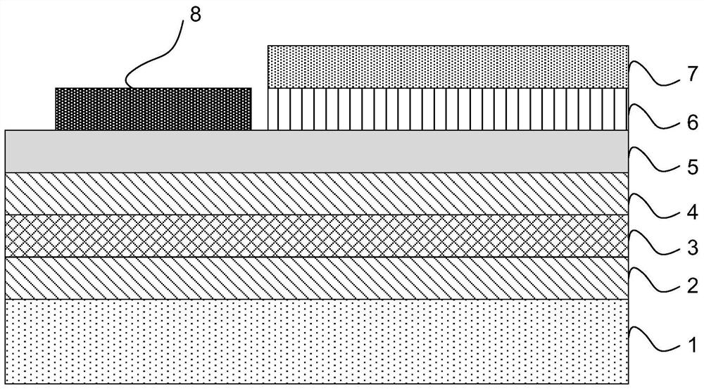
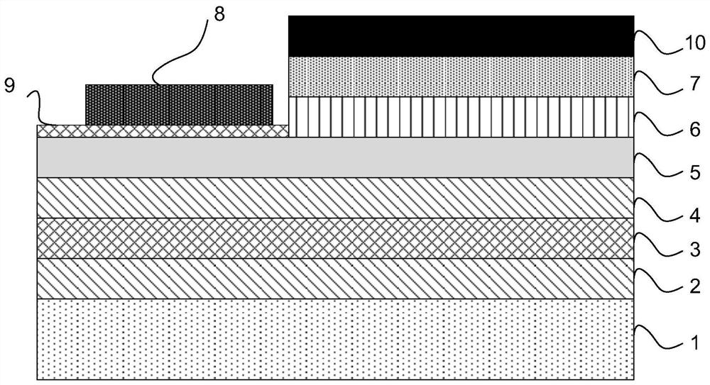
[0033] As mentioned in the background section, there is a contradiction between the high-frequency bandwidth and the device responsivity in the prior art, and it is impossible to obtain a device with high responsivity and high-frequency bandwidth.

[0034] The inventors found that the reason for the above phenomenon is that in order to make the photodetector have a higher bandwidth, the thickness of the absorbing layer needs to be thinner and thinner, and the thinning of the absorbing layer means that the light incident light path is shorter, resulting in a higher degree of device responsivity. The lower, that is, the high-frequency bandwidth and high responsivity of the photodetector are a pair of contradictions.

[0035] In order to solve the contradiction between high frequency bandwidth and device responsivity, waveguide photodetectors and resonant cavity enhanced (RCE) photodetectors are proposed in the prior art. However, RCE photodetectors have complex fabrication proce...


PUM

PropertyMeasurementUnit
Thicknessaaaaaaaaaa
Heightaaaaaaaaaa

Abstract

The invention provides a uni-traveling carrier photoelectric detector and a manufacturing method thereof. According to the invention, by introducing a surface plasmon structure near an absorption layer, the absorption of the absorption layer is increased by utilizing the characteristics of local field enhancement, near-field enhancement and scattering in transmission and the like to improve the photoelectric conversion efficiency of the absorption layer, so that the absorption layer with small thickness has high absorption performance, and the uni-traveling carrier photoelectric detector can also have a high responsivity characteristic on the absorption layer with a thin thickness; and with the method, in the design process of a high-speed uni-traveling carrier detector, the thickness of the absorption layer can be reduced on the premise of not sacrificing responsivity characteristic indexes of the device, so that the carrier transit time of the device is shortened, the high-frequencybandwidth characteristic of the device is improved, and the device with high responsivity and high-frequency bandwidth characteristic is realized at the same time.

Description

technical field [0001] The invention relates to the technical field of photoelectric detection, in particular to a single row carrier photodetector and a manufacturing method thereof. Background technique [0002] With the rapid development of photodetectors for high-speed optical communications, the photodetectors that play an important role are being designed towards higher efficiency and higher bandwidth. As a photodetector based on the internal photoelectric effect, semiconductor photodiodes have become the main type of photodetectors used in optical communication systems due to their small size, low noise, fast detection speed and high detection efficiency. [0003] The photodiode based on InGaAs material with an energy band of 0.73eV is currently the most widely used commercial optical communication photodetector in the optical communication waveguide 1550nm. As the most typical and widely used p-i-n type detector among photodetectors, it has lower dark current and qu...

Claims


Application Information

Patent Timeline
IPC IPC(8): H01L31/0216H01L31/105H01L31/18
CPCH01L31/105H01L31/02161H01L31/1844Y02E10/544
Inventor 张博健王亮王方莉郭松坡
Owner UNIV OF SCI & TECH OF CHINA
Why Eureka
Try Eureka