All-optical diffraction neural network and system implemented on optical waveguide and/or optical chip

A neural network and light diffraction technology, applied in the direction of optical waveguide light guide, optical waveguide coupling, multiplexing system selection device, etc., can solve the calculation rate and loss limited electrical clock rate and ohmic loss, cascade time Problems such as error amplification and limited scalability can be solved to achieve the effects of improved controllability, good fault tolerance and strong scalability

Active Publication Date: 2020-09-18
XI'AN INST OF OPTICS & FINE MECHANICS - CHINESE ACAD OF SCI +1
View PDF5 Cites 8 Cited by
  • Summary
  • Abstract
  • Description
  • Claims
  • Application Information

AI Technical Summary

Problems solved by technology

[0003] In order to solve the calculation rate and loss of the optical hybrid system is still limited by the rate and ohmic loss of the electrical clock, and the existing all-optical neural network system using discrete optical components has high

Method used


Image

  • All-optical diffraction neural network and system implemented on optical waveguide and/or optical chip
  • All-optical diffraction neural network and system implemented on optical waveguide and/or optical chip
  • All-optical diffraction neural network and system implemented on optical waveguide and/or optical chip

Examples


example 1

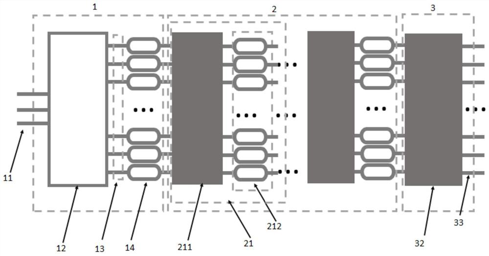
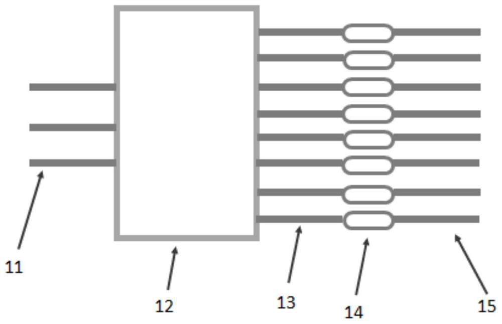
[0074] Such as Figure 11 As shown, the plenoptic diffraction neural network provided in this example has the function of image classification and recognition, and the network structure includes an input layer 1 , a network layer 2 composed of two sub-network layers 21 and an output layer 3 . This optical network structure is realized based on passive integrated optical waveguide. The input layer 1 of this example is composed of an input layer input waveguide 11, an optical splitter 12 (this example is realized by a light diffraction free transmission area), a group of input layer array amplitude-phase modulators 14 (this example is a passive amplitude value modulator, realized by truncating the waveguide) and a set of input layer array output waveguides 15. The coherent light enters the all-optical diffraction neural network from the input port of the input layer 1, and divides 1 path of light into 128 paths of light through the light diffraction free transmission area and ou...

example 2

[0076] Such as Figure 12 As shown, the all-optical diffraction neural network provided in this example has the function of vowel classification and recognition. The network structure includes an input layer 1, a network layer 2 composed of four cascaded sub-network layers, and an output layer 3. This optical network is based on active integrated optical waveguides. In this example, there are two types of length differences between the arrayed waveguides connecting the input layer 1 and the network layer 2, and each sub-network layer, which are 0 μm and 11.2 μm. Among them, the length difference between two adjacent waveguides in the arrayed waveguide between the input layer 1 and the first sub-network layer, the length of two adjacent waveguides in the arrayed waveguide between the first sub-network layer and the second sub-network layer difference, the length difference between two adjacent waveguides in the array waveguide between the 3rd sub-network layer and the 4th sub-...


PUM


Abstract

In order to solve the technical problem that the calculation rate and loss of a photoelectric hybrid system are still limited by the rate and ohmic loss of an electric clock, and the high cost, largesize, limited expansibility and amplification of errors during cascading of a conventional all-optical neural network system implemented by using discrete optical elements, the invention provides an all-optical diffraction neural network and system implemented on an optical waveguide and/or an optical chip. All-optical connection is realized through the diffraction free transmission region on theoptical waveguide and/or the chip, and more waveguide neuronal connections can be realized under the same size, so that the problems of few neuronal connections and weak system expansion can be effectively solved; and more neuronal connection error-tolerant rates are better, so that the method is higher in recognition precision.

Description

Background technique [0001] With the development of big data, cloud computing, and the Internet of Things, and the development and promotion of artificial intelligence computers with perception, learning, and decision-making, the volume of data in the future will explode. Modern computers based on the von Neumann structure have a wide range of applications in computing, perception, communication, learning, and decision-making. However, compared with their corresponding biological structures, the central nervous system, they consume more power and have weaker computing power. In the future, in the fields of big data, cloud computing, Internet of Things, and artificial intelligence, low power consumption, fast and effective analysis of data will become the focus of more and more attention. For example, there will be more and more applications in real-time processing of images in specific fields, and online recognition and response of voice information uploaded from mobile phones...

Claims


Application Information

Patent Timeline
IPC IPC(8): H04Q11/00G02B6/12G02B6/26
CPCH04Q11/0062H04Q11/0071G02B6/12G02B6/26
Inventor 赵卫程东杜炳政布兰特·埃弗雷特·李特尔谢小平罗伊·戴维森王翔李伟恒姚宏鹏范修宏
Owner XI'AN INST OF OPTICS & FINE MECHANICS - CHINESE ACAD OF SCI
Why Eureka
Try Eureka