SiC trench gate power MOSFET device and preparation method thereof

A trench gate and trench technology, which is applied in semiconductor/solid-state device manufacturing, semiconductor devices, electrical components, etc., to achieve the effects of reducing conduction voltage drop, increasing chip area, and reducing switching loss

Active Publication Date: 2020-09-22
HANGZHOU SILICON-MAGIC SEMICON TECH CO LTD
View PDF6 Cites 13 Cited by
  • Summary
  • Abstract
  • Description
  • Claims
  • Application Information

AI Technical Summary

Problems solved by technology

[0003] The technical problem to be solved by the present invention is to provide a SiC trench gate power MOSFET device and its preparation method for the existing SiC power MOSFET device structure using parasitic PIN diodes or external diodes.

Method used


Image

  • SiC trench gate power MOSFET device and preparation method thereof
  • SiC trench gate power MOSFET device and preparation method thereof
  • SiC trench gate power MOSFET device and preparation method thereof

Examples


Embodiment Construction

[0064] The principles and features of the present invention are described below in conjunction with the accompanying drawings, and the examples given are only used to explain the present invention, and are not intended to limit the scope of the present invention.

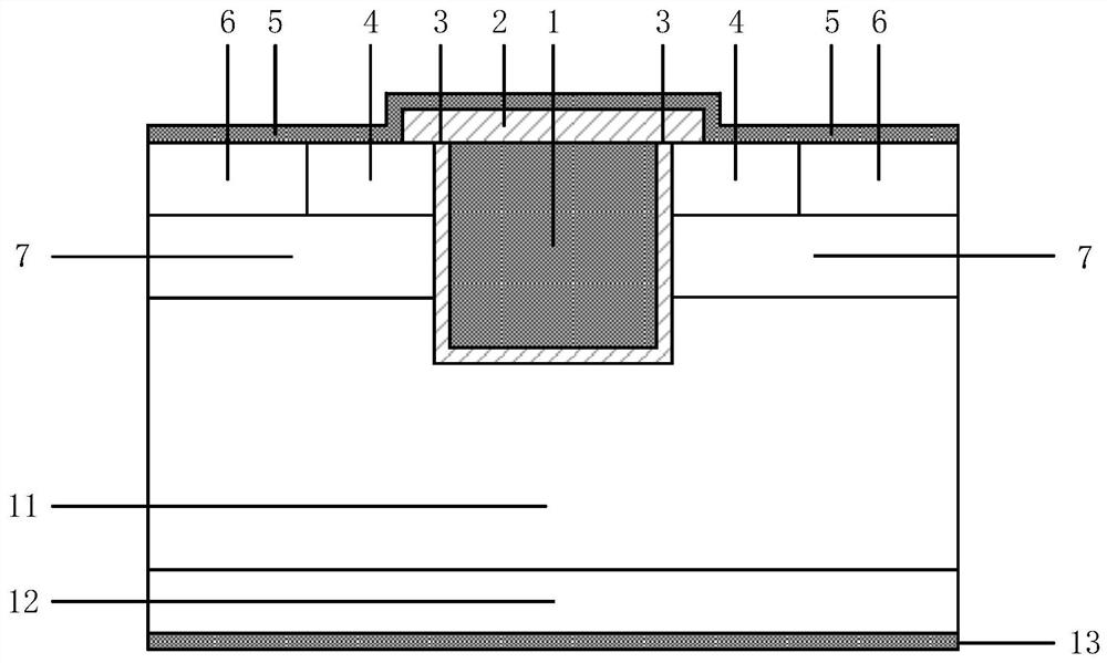
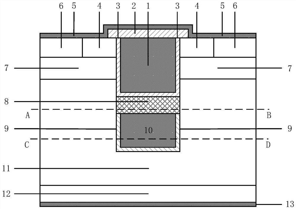
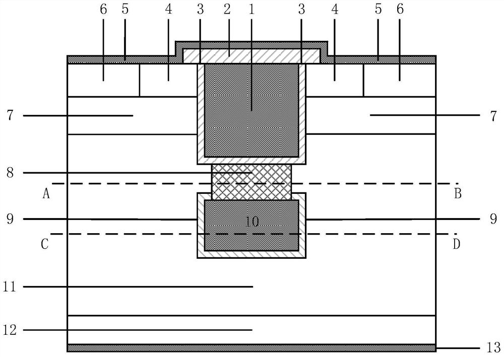
[0065] Such as figure 2 As shown, a SiC trench gate power MOSFET device provided in Embodiment 1 of the present invention has a cell structure including metallized drain 13, N+ drain region 12, N-drift region 11 and metal source electrode 5;

[0066] The N-drift region 11 has a trench source structure, a P-type polysilicon 8, a trench gate structure, a P-type base region 7, a P+ low-resistivity region 6 and an N+ source region 4;

[0067] The trench source structure, P-type polysilicon 8 and trench gate structure are sequentially stacked on the top layer of the N-drift region 11 from bottom to top; the P-type base region 7 is located on both sides of the trench gate structure , the sides of the P+ low-resistivity...


PUM

PropertyMeasurementUnit
thicknessaaaaaaaaaa
depthaaaaaaaaaa
thicknessaaaaaaaaaa

Abstract

The invention relates to a SiC trench gate power MOSFET device, and belongs to the technical field of power semiconductors. The SiC trench gate power MOSFET device comprises a trench source structure,a P-type polycrystalline silicon and a trench gate structure which are manufactured in a trench. The trench source structure can reduce gate-drain capacitance (Cgd) and switching loss, when a sourcedielectric layer is made of a high-K dielectric material, the electric field intensity of a source dielectric can be effectively reduced, the P-type polycrystalline silicon realizes integration of anHJD in the N-channel SiC trench gate power MOSFET, the HJD has lower forward conduction voltage drop, conduction of a body diode is inhibited, a reliability problem caused by bipolar degradation is avoided, and the integrated HJD does not additionally increase the area of a chip. The integrated SiCHJD is a unipolar device, the reverse recovery characteristic is superior to that of a bipolar body diode, and stability is better due to the fact that parasitic parameters brought by an external diode lead are avoided, in addition, the device is simple and controllable in manufacturing process and high in compatibility with an existing process.

Description

technical field [0001] The invention belongs to the technical field of power semiconductors, and in particular relates to a SiC trench gate power MOSFET device and a preparation method thereof. Background technique [0002] Silicon carbide (Silicon carbide, chemical formula SiC) trench gate power metal oxide semiconductor field effect transistor (Metal Oxide Semiconductor Field Effect Transistor, referred to as MOSFET) has a smaller size than traditional silicon-based power MOSFETs due to the excellent performance of SiC materials. On-resistance, higher operating temperature and stronger radiation resistance. In addition, the power MOSFET is a unipolar device without minority carrier injection. Compared with the bipolar device - Insulated Gate Bipolar Transistor (IGBT) has faster switching speed and lower switching losses. figure 1 The cell structure of a conventional SiC power MOSFET is shown. In practical applications, the power MOSFET needs to be used in conjunction wi...

Claims


Application Information

Patent Timeline
Patent Type & Authority Applications(China)
IPC IPC(8): H01L29/78H01L29/417H01L21/336
CPCH01L29/7805H01L29/7813H01L29/41741H01L29/41775H01L29/66068
Inventor 张金平陈子珣涂元元刘竞秀张波
Owner HANGZHOU SILICON-MAGIC SEMICON TECH CO LTD
Why Eureka
Try Eureka