Chip packaging preprocessing method and chip analysis method

A multi-chip packaging and pretreatment technology, applied in chemical instruments and methods, electrical components, semiconductor/solid-state device manufacturing, etc., can solve problems such as difficulty in removing the bare die to be removed, and overcome FIB pretreatment problems and costs. Inexpensive, easy-to-use effects

Pending Publication Date: 2020-09-25
BEIJING CHIP IDENTIFICATION TECH CO LTD +2
View PDF8 Cites 5 Cited by
  • Summary
  • Abstract
  • Description
  • Claims
  • Application Information

AI Technical Summary

Problems solved by technology

[0008] The purpose of the present invention is to provide a chip packaging pretreatment method and a chip analysis method to solve technical problems such as difficult to remove the bare die to be removed and retain the intact target die before chip analysis

Method used


Image

  • Chip packaging preprocessing method and chip analysis method
  • Chip packaging preprocessing method and chip analysis method
  • Chip packaging preprocessing method and chip analysis method

Examples


Embodiment 1

[0067] An embodiment of the present invention provides a preprocessing method for multi-chip packaging, and the preprocessing method may include:

[0068] Detect the surface projection area of ​​different die on the multi-chip package;

[0069] Protection of multi-chip packages outside the projected area of ​​the surface from which the die is to be removed;

[0070] etching the multi-chip package;

[0071] peeling off the die to be removed to obtain a bare target die.

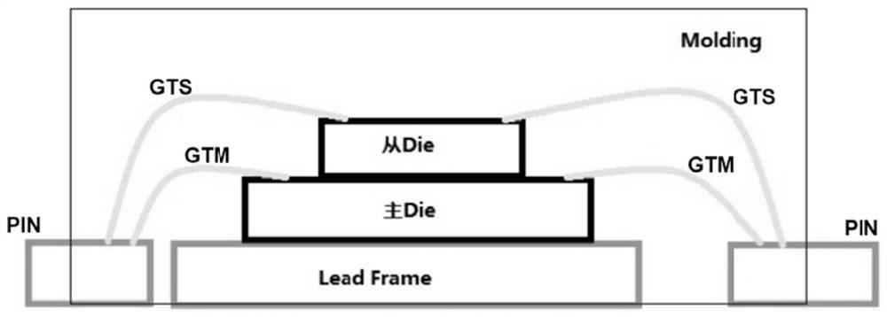
[0072] Such as figure 1 , the chips to be preprocessed are stacked and packaged, called multi-chip packaging, from Die is the bare die to be removed, the main Die is the target bare die, LeadFrame is the lead frame, Molding is molding, and molding is usually resin Constituted, GTS is the gold wire of the slave Die, GTM is the gold wire of the main Die, PIN is the outer pin of the package, and the surface projection area can be projected onto the molded outer surface of the chip with the surface of the lead f...

Embodiment 2

[0100] Based on Embodiment 1, the embodiment of the present invention provides a chip analysis method, which includes:

[0101] Perform the preprocessing method described in Embodiment 1 on the chip;

[0102] Focused ion beam analysis was performed on the preconditioned chip.

[0103] Further, exemplarily, performing focused ion beam (FIB) analysis on the pre-processed chip may include:

[0104] Using a FIB device to generate a focused ion beam to irradiate the main Die of the pretreated chip or a Die sample extracted from the pretreated chip, wherein the Die sample or the main Die responds to a charge pulse corresponding to the ion beam;

[0105] The charge pulse is received by a spectrum amplifier, and the output wave of the spectrum amplifier corresponding to the charge pulse is received by a multi-channel analyzer, thereby realizing failure analysis of the main Die or the Die sample.


PUM


Abstract

The invention provides a chip packaging preprocessing method and a chip analysis method, and belongs to the technical field of integrated circuits. The preprocessing method comprises the following steps of detecting the projection areas of different bare dies on the surface of the multi-chip package; protecting the multi-chip package outside the surface projection area of the bare chip to be removed; corroding the multi-chip package; and stripping the bare die to be removed to obtain an exposed target bare die. The methods are used for FIB pretreatment.

Description

technical field [0001] The invention relates to the technical field of integrated circuits, in particular to a pretreatment method for multi-chip packaging, a reaction adhesion medium solution, a gold corrosion solution and a chip analysis method. Background technique [0002] As the chip integration becomes higher and higher, there are usually two or more chips inside the chip package. In order to save the chip area, a stacked package is usually used. [0003] In chip failure analysis and chip revision testing, most of them need to use FIB (Focused Ion Beam) to analyze chip failure mechanism and chip circuit repair. In a multi-chip package, the master Die (main die) is the core chip, and the slave die (slave die) are mostly auxiliary chips such as storage and switches. FIB preprocessing is a means to maintain chip pin connectivity and expose all chips under test. In the multi-chip package, since the slave Die is bonded to the main Die, most of the area of ​​the main Die i...

Claims


Application Information

Patent Timeline
Patent Type & Authority Applications(China)
IPC IPC(8): H01L21/67H01L21/66C09K13/00
CPCH01L21/67126H01L21/67092H01L22/12C09K13/00
Inventor 单书珊钟明琛陈燕宁
Owner BEIJING CHIP IDENTIFICATION TECH CO LTD
Why Eureka
Try Eureka