Unlock instant, AI-driven research and patent intelligence for your innovation.

Silicon carbide single crystal growth device

A silicon carbide single crystal and growth device technology, applied in the directions of single crystal growth, single crystal growth, crystal growth, etc., can solve the problems that are not conducive to the preparation of silicon carbide crystals, uneven distribution of gas phase components, uneven radial heat transfer, etc. problems, to achieve the effect of reducing impurities and defects, improving crystal quality, and heating uniformly

Active Publication Date: 2020-10-09
BEIJING NAURA MICROELECTRONICS EQUIP CO LTD
View PDF3 Cites 8 Cited by
  • Summary
  • Abstract
  • Description
  • Claims
  • Application Information

AI Technical Summary

Problems solved by technology

The uneven radial heat transfer of the crucible can easily lead to uneven distribution of the thermal field, resulting in uneven distribution of gas phase components, resulting in different concentrations of components on the radial distribution of the seed crystal surface, which is not conducive to the preparation of high-quality silicon carbide crystals

Method used


Image

  • Silicon carbide single crystal growth device
  • Silicon carbide single crystal growth device
  • Silicon carbide single crystal growth device

Examples


Embodiment Construction

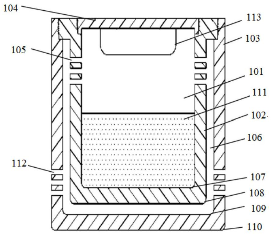
[0034] Such as figure 1 As shown, an existing silicon carbide single crystal growth device includes: a chamber 101, a first wall 102, a second wall 103, a cover 104, a plurality of first openings 105, a first space 106, a first Inner bottom corner 107 of the layer wall, outer bottom corner 108 of the first layer wall, inner bottom corner 109 of the second layer wall, outer bottom corner 110 of the second layer wall, material 111, second opening 112 and grown silicon carbide single crystal 113 . The purpose of this device is to pass through high-purity silane by setting the second opening 112 and the first opening 105, and react with the remaining fluffy carbon powder after carbonization to form silicon carbide powder again, so as to realize the continuous growth of single crystal and improve the crystal quality .

[0035] In this device, high-purity silane gas is introduced from the outside by setting the first opening 105 and the second opening 112, and the gas passage need...


PUM


Abstract

The invention discloses a silicon carbide single crystal growth device, which comprises: a graphite crucible for containing a silicon carbide powder material and heating the silicon carbide powder material to sublimate and decompose the silicon carbide powder material into a gas phase component, a seed crystal support for containing seed crystals capable of growing silicon carbide single crystals,and a heat conduction container comprising a container wall and a cavity, wherein the heat conduction container is arranged in the graphite crucible, the cavity is used for containing silicon-containing powder and the container wall is used for conducting heat of the graphite crucible into the cavity, so that a gas-phase component generated after the silicon-containing powder absorbs the heat canbe slowly released into the silicon carbide powder in the graphite crucible. Gas-phase silicon components are supplemented in the silicon carbide single crystal growth process, the ratio of carbon tosilicon components in a crystal growth area is kept unchanged while silicon carbide powder carbonization is reduced, the defects of carbon inclusions in the silicon carbide single crystal are reduced, and the growth quality of the silicon carbide single crystal is improved.

Description

technical field [0001] The invention relates to the technical field of semiconductor equipment, and more specifically, to a silicon carbide single crystal growth device. Background technique [0002] Silicon carbide SiC belongs to the third generation of semiconductor materials. It has the characteristics of wide bandgap, high thermal conductivity, high critical breakdown field, and high electron saturation drift rate. It is a popular material for preparing high-temperature, high-frequency, and high-power devices. Automobiles, high-speed rail, communications, aerospace and other fields have broad prospects. [0003] The current silicon carbide single crystal growth technologies mainly include physical vapor transport (PVT), liquid phase epitaxy (LPE) and chemical vapor deposition (CVD). Among them, PVT technology has been widely used. Its principle is to heat the graphite crucible placed in the coil through medium frequency induction heating, and form an axial temperature g...

Claims


Application Information

Patent Timeline
IPC IPC(8): C30B23/00C30B29/36
CPCC30B23/00C30B29/36
Inventor 崔殿鹏
Owner BEIJING NAURA MICROELECTRONICS EQUIP CO LTD
Features
  • R&D
  • Intellectual Property
  • Life Sciences
  • Materials
  • Tech Scout
  • Unparalleled Data Quality
  • Higher Quality Content
  • 60% Fewer Hallucinations
Learn More