

Asymmetric-structure high-power laser with Bragg reflector and preparation method thereof
A technology of high-power lasers and Bragg mirrors, applied in the field of lasers, can solve problems such as internal quantum efficiency reduction, working temperature sensitivity, and sensitive memory effects
- Summary
- Abstract
- Description
- Claims
- Application Information
AI Technical Summary
Problems solved by technology
Method used
Image

Examples
Embodiment 1
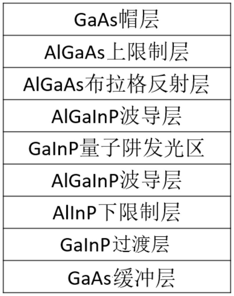
[0056] An asymmetric high-power laser with a Bragg reflector, such as figure 1 As shown, the GaAs substrate is included, and the GaAs buffer layer, GaAs buffer layer, Ga 1-x In x P transition layer, Al 1-x In x P lower confinement layer, (Al 1-x Ga x ) y In 1-y P lower waveguide layer, Ga 1-x In x P quantum well light-emitting region, (Al 1-x Ga x ) y In 1-y P upper waveguide layer, Al 1-x Ga x As Bragg reflector, Al 1-x Ga x As upper confinement layer and GaAs cap layer.
Embodiment 2
[0058] A kind of asymmetric structure high-power laser with Bragg reflector, structure as shown in embodiment 1, difference is, (Al 1-x Ga x ) y In 1-y The thickness of the waveguide layer under P is related to (Al 1-x Ga x ) y In 1-y The waveguide layers on P have different thicknesses, preferably 0.12 μm and 0.07 μm respectively.
Embodiment 3
[0060] A preparation method of an asymmetric structure high-power laser with a Bragg reflector, comprising the steps of:
[0061] (1) Put GaAs substrate in MOCVD equipment, H 2 The environment is heated to 720±10°C and baked for 30 minutes, and AsH is introduced 3 , remove water and oxygen on the surface of the GaAs substrate to complete the surface heat treatment, and prepare for step (2);
[0062] (2) Slowly lower the temperature to 700±10°C, and continue to feed TMGa and AsH 3 , grow a GaAs buffer layer with a thickness of 0.3 μm on the GaAs substrate;
[0063] (3) Keep the temperature at 700±10°C, continue to feed TMIn, TMGa and PH 3 , grow Ga on the GaAs buffer layer in step (2) 1-x In x P transition layer;
[0064] (4) Keep the temperature at 700±10°C, continue to feed TMIn, TMAl and PH 3 , Ga in step (3) 1-x In x Growth of n-type Al on P transition layer 1-x In x P lower limit layer;
[0065] (5) The temperature is lowered to 650±10°C, and TMIn, TMAl, TMGa a...
PUM
| Property | Measurement | Unit |
|---|---|---|
| thickness | aaaaa | aaaaa |
| thickness | aaaaa | aaaaa |
| thickness | aaaaa | aaaaa |
Abstract
Description
Claims
Application Information