Method of manufacturing insulating circuit board with heat sink

A technology for circuit substrates and manufacturing methods, which is applied in semiconductor/solid-state device manufacturing, circuits, manufacturing tools, etc., and can solve the problems of reduced reliability of bonding between metal layers and heat sinks, insufficient solid-phase diffusion, and high activation energy of 4N aluminum

Pending Publication Date: 2020-10-20
MITSUBISHI MATERIALS CORP
View PDF4 Cites 0 Cited by
  • Summary
  • Abstract
  • Description
  • Claims
  • Application Information

AI Technical Summary

Problems solved by technology

[0015] When the metal layer is composed of 4N aluminum, and the bonding surface of the heat sink is composed of an aluminum alloy such as ADC12, when they are solid-phase diffusion bonded by the method described in Patent Document 3, due to the solid state of the metal layer and the bonding surface of the heat sink, The difference in phase line temperature is large, so it is necessary to set the temperature condition during solid phase diffusion bonding to be lower than the solidus temperature of aluminum alloy, and because the activation energy of diffusion of high-purity 4N aluminum is high, it is difficult to cause diffusion phenomenon, so In some cases, the solid-state diffusion of Al in the metal layer formed of 4N aluminum with a high solidus temperature and Cu in the bonding material becomes insufficient, resulting in a decrease in the bonding reliability between the metal layer and the heat sink

Method used


Image

  • Method of manufacturing insulating circuit board with heat sink
  • Method of manufacturing insulating circuit board with heat sink
  • Method of manufacturing insulating circuit board with heat sink

Examples


Embodiment

[0114] A confirmation experiment conducted to confirm the effectiveness of the present invention will be described below.

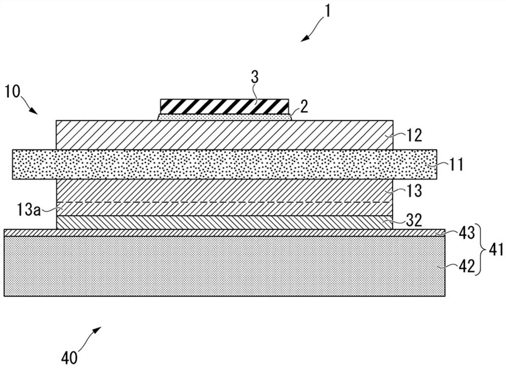
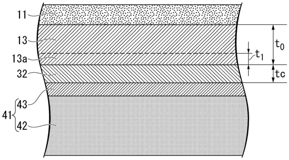
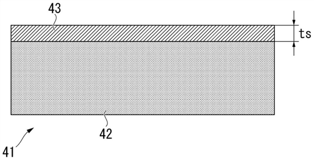
[0115] A circuit layer (37mm×37mm×thickness 0.4mm) made of aluminum (4N aluminum) with a purity of 99.99 mass% or more is formed on one surface of a ceramic substrate (40mm×40mm×thickness 0.635mm) made of aluminum nitride (AlN) , and a metal layer (37mm×37mm) of the material and thickness shown in Table 1 was formed on the other surface of the ceramic substrate. Al-7.5 mass %Si-0.01 mass %Mg brazing filler metal foil (thickness 15 micrometers) was used for bonding the ceramic substrate and the aluminum plate used as a circuit layer and a metal layer.

[0116] Then, the clad material having the structure shown in Table 1 was laminated on the surface of the aluminum plate serving as the metal layer on the opposite side to the ceramic substrate.

[0117] Then, heat treatment was performed according to the conditions shown in Table 1.

[0118] Then, a heat ...


PUM

PropertyMeasurementUnit
thicknessaaaaaaaaaa
thicknessaaaaaaaaaa
thicknessaaaaaaaaaa

Abstract

A method of manufacturing an insulating circuit board with heat sink which is provided with an insulating circuit board and a heat sink bonded to the metal layer side of the insulating circuit board.The metal layer is configured from aluminum. The heat sink has a surface for bonding with the insulating circuit board which is configured from an aluminum alloy having a solidus temperature of less than or equal to 650 DEG C. The method is provided with: an alloy element high-concentration portion forming step (S02) of forming an alloy element high-concentration portion; and a heat sink bonding step (S03) of bonding the heat sink. The ratio tb/ta of a thickness ta of a core material of the cladding material and a thickness tb of the thickness of a brazing material layer is in a range of from0.1 to 0.3 inclusive.

Description

technical field [0001] The present invention relates to a method of manufacturing an insulated circuit substrate with a heat sink. The insulated circuit substrate with a heat sink has a circuit layer formed on one surface of an insulating layer and a metal layer formed on the other surface of the insulating layer. An insulating circuit substrate, and a heat sink bonded to the metal layer side of the insulating circuit substrate. [0002] This application claims priority based on Patent Application No. 2018-059917 filed in Japan on March 27, 2018, and uses the content thereof here. Background technique [0003] In a power module, an LED module, and a thermoelectric module, a structure is made in which a power semiconductor element, an LED element, and a thermoelectric element are bonded to an insulating circuit substrate, and a conductive material is formed on one surface of an insulating layer of the insulating circuit substrate. formed circuit layers. [0004] For example...

Claims


Application Information

Patent Timeline
Patent Type & Authority Applications(China)
IPC IPC(8): H01L23/36B23K20/00H01L23/12
CPCH01L23/12H01L2224/32225H01L21/4882H01L23/3735H01L23/3736C04B37/021C04B2237/365C04B2237/368C04B2237/343C04B2237/366C04B2237/402H01L23/142H01L23/367B23K20/00H01L23/36H01L2924/14
Inventor 北原丈嗣长友义幸
Owner MITSUBISHI MATERIALS CORP
Why Eureka
Try Eureka