
Multilayer thin film electrode, HF transmission line, HF resonator and HF filter

A multi-layer film and resonator technology, applied in circuits, resonators, waveguides, etc., can solve the problems of reduced reliability, low adhesion strength, and unsatisfactory suppression of skin effect

Inactive Publication Date: 2003-08-13
MURATA MFG CO LTD
View PDF4 Cites 0 Cited by
  • Summary
  • Abstract
  • Description
  • Claims
  • Application Information

AI Technical Summary

Problems solved by technology

[0009] However, such existing multilayer thin-film electrodes have disadvantages of low adhesion strength between the dielectric substrate and its adjacent thin conductive film, and between each thin dielectric film and its adjacent thin conductive film, resulting in low reliability. reduce
Furthermore, in order to improve the adhesive strength between the dielectric substrate and its adjacent thin conductive film, between each thin dielectric film and its adjacent thin conductive film, when an adhesive conductive film is provided between layers, Unsatisfactory suppression of skin effect

Method used


Image

  • Multilayer thin film electrode, HF transmission line, HF resonator and HF filter
  • Multilayer thin film electrode, HF transmission line, HF resonator and HF filter
  • Multilayer thin film electrode, HF transmission line, HF resonator and HF filter

Examples


Embodiment 1

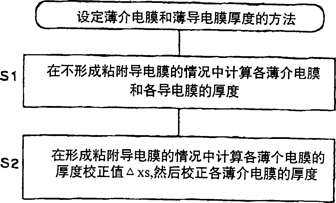
[0064] For comparison, first, the results obtained from the evaluation of the conventional multilayer thin film electrodes will be described, and second, the results of Example 1 will be described. Table 2 provides the obtained result to the evaluation of existing multilayer thin film electrode, and this multilayer thin film electrode has five layers of thin conductive film layers (the number of film layers refers to the number of thin conductive film layers in the future), under the above-mentioned parameter conditions , no adhesive conductive film was formed.

[0065] Table 2 sets the film thickness and Q rise rate of existing multilayer thin film electrodes (5 layers)

[0066] Thickness of thin conductive film 1 4.2 μm (top layer)

[0067] Thickness of other thin conductive film 1: 0.756 μm

[0068] Thickness of thin dielectric film 0.0968μm

[0069] Q increase rate 2.39 times

[0070]In the existing multilayer thin film electrodes shown in Table 2, when between the die...

Embodiment 2

[0079] In Example 2, the Q rise rate of a multilayer thin film electrode having ten layers, which was prepared according to the same parameters as in Example 1, was evaluated. Table 4 shows the thickness and Q rise rate of setting the existing multilayer thin film electrodes. Table 5 shows the thickness and Q rise rate of the multilayer thin film electrode of Setting Example 2, which provides an adhesive conductive film, and corrects the thickness of each thin dielectric film to a predetermined thickness.

[0080] Table 4 sets the film thickness and Q rise rate of existing multilayer thin film electrodes (10 layers)

[0081] Thickness of thin conductive film 1 4.2 μm (top layer)

[0082] Thickness of other thin conductive film 1: 0.556 μm

[0083] Thickness of thin dielectric film 0.0686μm

[0084] Q increase rate 3.33 times

[0085] Table 5 sets the film thickness and Q rise rate of embodiment 2 multilayer thin film electrode (10 layers)

[0086] Thickness of thin conduc...


PUM

PropertyMeasurementUnit
Thicknessaaaaaaaaaa
Thicknessaaaaaaaaaa
Thicknessaaaaaaaaaa

Abstract

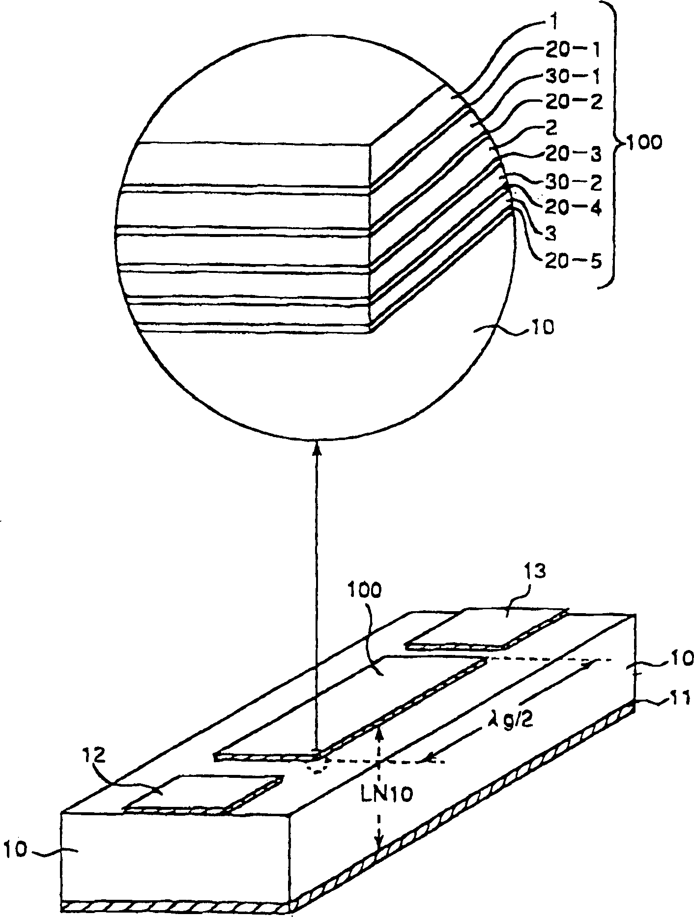
A multi-layer thin-film electrode comprises thin conductor films and thin dielectric films each being alternately laminated on a dielectric substrate, in which an electro-magnetic field generated in the dielectric substrate and that generated in each of the thin dielectric films have substantially the same phase at a predetermined frequency. According to the multi-layer thin-film electrode of the present invention, adhesive conductor films that more easily form metallic oxide as compared with the thin conductor films are provided between the dielectric substrate and the thin conductor films adjacent thereto and between each of the thin conductor films and the thin dielectric film adjacent thereto, respectively, and an increase in the surface reactance of the thin conductor films caused by the adhesive conductor film formation is canceled by correcting the thickness of each of the thin dielectric films based on the dielectric constant of the thin dielectric film and the dielectric substrate and the thickness of at least one of the adhesive conductor films.

Description

(1) Technical field [0001] The invention relates to a multilayer film electrode used in high-frequency bands such as microwave, submillimeter wave or millimeter wave. (2) Background technology [0002] Recently, the size of electronic components has been reduced. The size of high-frequency devices used in high-frequency bands such as microwaves, submillimeter waves, or millimeter waves is also reduced by using materials with high dielectric constants. However, when achieving a smaller size by increasing the dielectric constant, there is a disadvantage of energy loss that is inversely proportional to the cube root of the volume. The energy loss of high-frequency devices can be roughly divided into conductor loss due to the skin effect and dielectric loss due to dielectric materials. Recently, dielectric materials with high dielectric constant and low dielectric loss have been put into practical use. Therefore, conductor losses are more dominant than dielectric losses in de...

Claims


Application Information

Patent Timeline
IPC IPC(8): H01P1/203H01P3/06H01P3/08H01P3/18H01P7/08
CPCH01P3/06H01P7/084H01P7/082H01P1/20363H01P3/088H01P3/18
Inventor 石川容平日高青路松井则文伊势智之
Owner MURATA MFG CO LTD
Learn More