Self-aligned GaN Schottky diode and manufacturing method thereof
A technology of Schottky diode and manufacturing method, applied in diode, semiconductor/solid-state device manufacturing, semiconductor device and other directions, can solve the problems of current crowding, low plane process compatibility, complex manufacturing process, etc.
- Summary
- Abstract
- Description
- Claims
- Application Information
AI Technical Summary
Problems solved by technology
Method used
Image
Examples
Embodiment 1
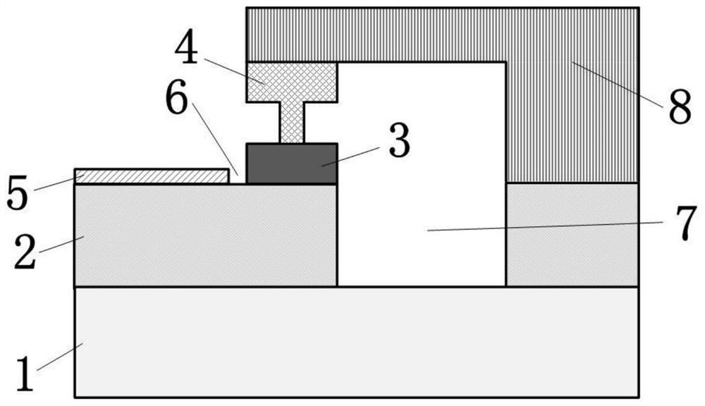
[0044] Example 1: Prepare a SiC substrate 1, the width of the spacer 6 is 150nm, the metal of the T-shaped anode 4 is Ni / Pt / Au, and the doping concentration of the n-GaN layer 3 is 2E17 / cm 3 , the doping concentration of n+GaN layer 2 is 5E19 / cm 3 Specifications of a self-aligned GaN Schottky diode, its fabrication process is:
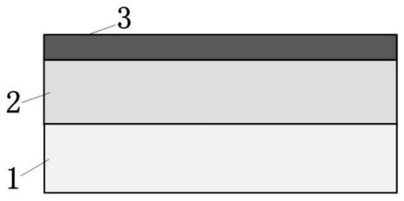
[0045] 1) On a SiC substrate 1, a 1 μm thick n+GaN layer 2 is grown at 950°C by metal organic chemical vapor deposition technique MOCVD, the doping source is Si, and the doping concentration is 5E19 / cm 3 , and then grow a 1μm thick n-GaN layer 3, the doping source is Si, and the doping concentration is 2E17 / cm 3 .
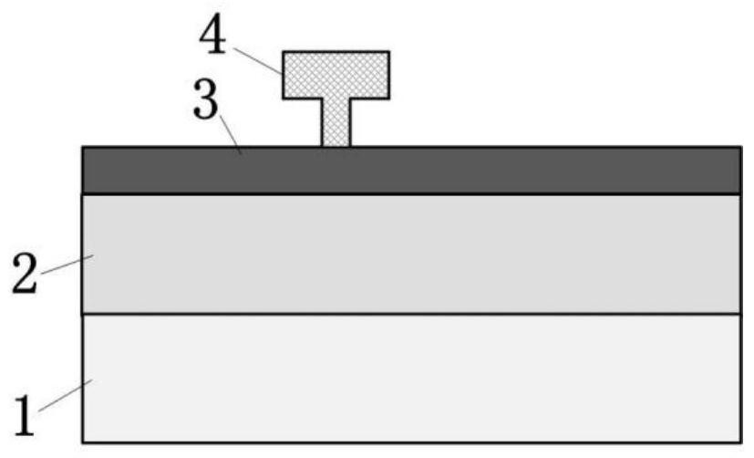
[0046] 2) Lithograph the anode pattern on the top of the n-GaN layer 3, and then use evaporated anode metal to peel off to form a T-shaped anode 4; the material of the evaporated anode metal is Ni, Pt and Au from bottom to top, and the thickness of the metal layer is respectively 30nm, 50nm and 600nm; the process conditions of electron b...
Embodiment 2
[0053] Example 2: Si substrate 1 is prepared, the width of spacer 6 is 20nm, the metal of T-type anode 4 is W / Ti / Au, and the doping concentration of n-GaN layer 3 is 5E17 / cm 3 , the doping concentration of n+GaN layer 2 is 4E20 / cm 3 Specifications of a self-aligned GaN Schottky diode, its fabrication process is:
[0054] 1) On the SiC substrate 1, a 2 μm thick n+GaN layer 2 is grown at 950°C by using the metal organic chemical vapor deposition technique MOCVD, the doping source is Ge, and the doping concentration is 4E20 / cm 3 , and then grow a 300nm thick n-GaN layer 3, the doping source is Ge, and the doping concentration is 5E17 / cm 3 .
[0055] 2) Lithograph the anode pattern on the top of the n-GaN layer 3, then sputter the anode metal, and peel off to form a T-shaped anode 4; the material of the evaporated anode metal is W, Ti and Au from bottom to top, and the thickness of the metal layer is respectively 20nm, 20nm and 700nm; the process conditions of magnetron sputter...
PUM
| Property | Measurement | Unit |
|---|---|---|
| Width | aaaaa | aaaaa |
| Thickness | aaaaa | aaaaa |
| Thickness | aaaaa | aaaaa |
Abstract
Description
Claims
Application Information


