Large-scale preparation and patterning method of two-dimensional material semiconductor film and two-dimensional material semiconductor film

A technology for large-scale preparation of two-dimensional materials, applied in the field of two-dimensional semiconductor thin film preparation, can solve the problems of inability to apply roll-to-roll technology, low resolution and precision, and uneven stacking of nanosheets

Active Publication Date: 2020-10-30
NANKAI UNIV
View PDF6 Cites 4 Cited by
  • Summary
  • Abstract
  • Description
  • Claims
  • Application Information

AI Technical Summary

Problems solved by technology

However, the solution-based two-dimensional semiconductor film assembly method still lacks a controllable film preparation process.
Although inkjet or spray printing can facilitate the patterning of semiconductor thin films, these printing proce

Method used


Image

  • Large-scale preparation and patterning method of two-dimensional material semiconductor film and two-dimensional material semiconductor film
  • Large-scale preparation and patterning method of two-dimensional material semiconductor film and two-dimensional material semiconductor film
  • Large-scale preparation and patterning method of two-dimensional material semiconductor film and two-dimensional material semiconductor film

Examples


Embodiment 1

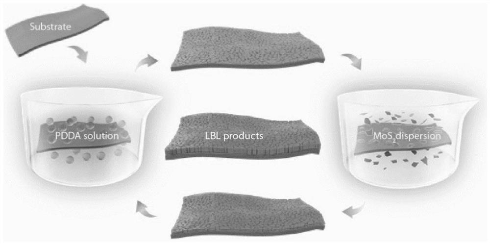
[0045] The invention discloses a large-scale preparation and patterning method of a two-dimensional material semiconductor thin film, comprising the following steps:

[0046] Step 1, pre-treat the substrate, the substrate can be rigid SiO 2 / Si or glass sheet, or flexible PET or PI, the specific operation is to ultrasonicate the substrate in acetone and isopropanol for 5 minutes, and then treat the substrate with oxygen plasma (120w, 5min).

[0047] Step 2, use a negative photolithography target pattern on the pretreated substrate: the specific operation is to spin coat the photoresist on the substrate (4000rpm, 30s); treat the substrate on a heating plate at 150°C for 1min; place the substrate on Under the mask plate of the target pattern of the lithography machine, expose it to a UV lamp for 10s; treat the substrate on a heating plate at 100°C for 1min; develop the substrate in the developer for 12s, clean the developer on the substrate with distilled water and dry it with a...

Embodiment 2

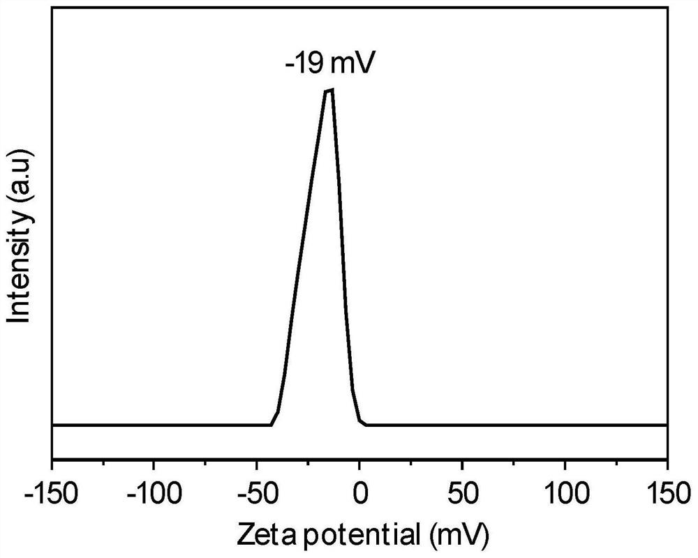
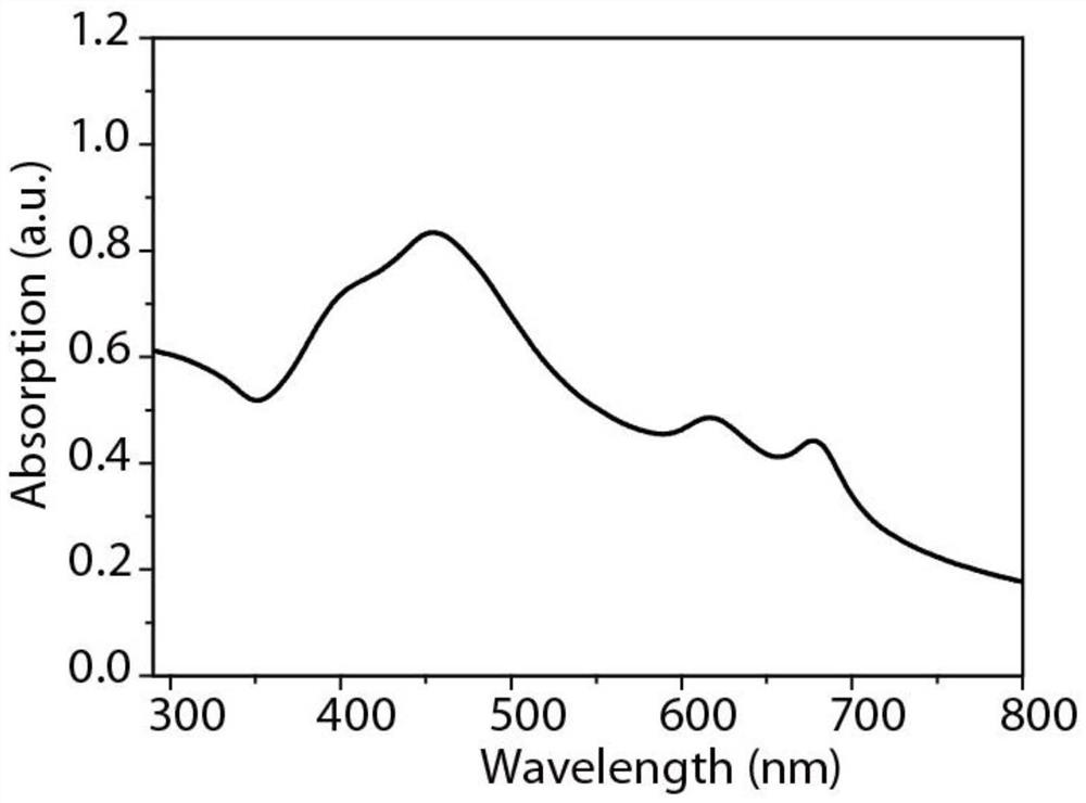
[0051] The solution self-assembly preparation and patterning method disclosed in the present invention can also be extended to other charged two-dimensional semiconductor materials, such as In 2 Se 3 two-dimensional semiconductor.

[0052] Step 1, pre-treat the substrate, the substrate can be rigid SiO 2 / Si or glass sheet, or flexible PET or PI, the specific operation is to ultrasonicate the substrate in acetone and isopropanol for 5 minutes, and then treat the substrate with oxygen plasma (120w, 5min).

[0053] Step 2, use a negative photolithography target pattern on the pretreated substrate: the specific operation is to spin coat the photoresist on the substrate (4000rpm, 30s); treat the substrate on a heating plate at 150°C for 1min; place the substrate on Under the mask plate of the target pattern of the lithography machine, expose it to a UV lamp for 10s; treat the substrate on a heating plate at 100°C for 1min; develop the substrate in the developer for 12s, clean th...


PUM


Abstract

The invention belongs to the technical field of two-dimensional semiconductor film preparation, and particularly relates to a large-scale preparation and patterning method of a two-dimensional material semiconductor film. The method comprises the following steps of pre-treating a substrate; photoetching a target pattern on the pretreated substrate by using negative photoresist; preparing a two-dimensional semiconductor film on the substrate with a photoresist pattern by using a solution self-assembly technology, wherein the substrate is firstly soaked in a poly(diallyldimethylammonium chloride) aqueous solution and then soaked in a MoS2 aqueous solution, and the process can be repeated for many times; and soaking the film obtained on the substrate in acetone to remove the photoresist, andfinally, obtaining the target MoS2 pattern. The method has the advantages that the preparation method is simple and can be operated on any substrate; the thickness of the film is controllable, and thepatterning can be realized; reaction conditions are mild, and the method has wide application space in the field of high-performance two-dimensional semiconductor film electronic devices.

Description

technical field [0001] The invention belongs to the technical field of two-dimensional semiconductor thin film preparation, and in particular relates to a large-scale preparation and patterning method of a two-dimensional material semiconductor thin film. Background technique [0002] The development of modern silicon-based semiconductor field has promoted the rapid development of microelectronics and optoelectronics technology. Semiconductor electronic devices are developing toward smaller, denser, faster, and more powerful information processing and storage and larger, lighter, cheaper, and more flexible information displays. [0003] Among numerous semiconductor materials, two-dimensional semiconducting thin films are more attractive in the field of thin film electronics due to their excellent charge transport and mechanical properties. However, the large-area preparation of uniform two-dimensional semiconductor thin films has been a challenge, which severely limits its ...

Claims


Application Information

Patent Timeline
IPC IPC(8): H01L21/368H01L29/24H01L29/786H01L21/34
CPCH01L21/02568H01L21/02628H01L21/02642H01L29/24H01L29/66969H01L29/786
Inventor 朱剑高香香尹君卞刚
Owner NANKAI UNIV
Why Eureka
Try Eureka