Junction Gate-Drain Power Devices

A leakage power and junction gate technology, applied in the field of microelectronics, can solve the problems of increasing device difficulty, high manufacturing cost, and reducing device yield

Active Publication Date: 2021-08-20
XIDIAN UNIV
View PDF4 Cites 0 Cited by
  • Summary
  • Abstract
  • Description
  • Claims
  • Application Information

AI Technical Summary

Problems solved by technology

However, the process of source-drain compound double-layer field plate power switching device is complicated, and the manufacturing cost is higher. The fabrication of each field plate requires process steps such as photolithography, metal deposition, and passivation medium deposition.
Moreover, in order to optimize the thickness of the dielectric material under the field plates of each layer to maximize the breakdown voltage, tedious process debugging and optimization must be carried out, which greatly increases the difficulty of device manufacturing and reduces the yield of devices.

Method used


Image

  • Junction Gate-Drain Power Devices
  • Junction Gate-Drain Power Devices
  • Junction Gate-Drain Power Devices

Examples


Embodiment 1

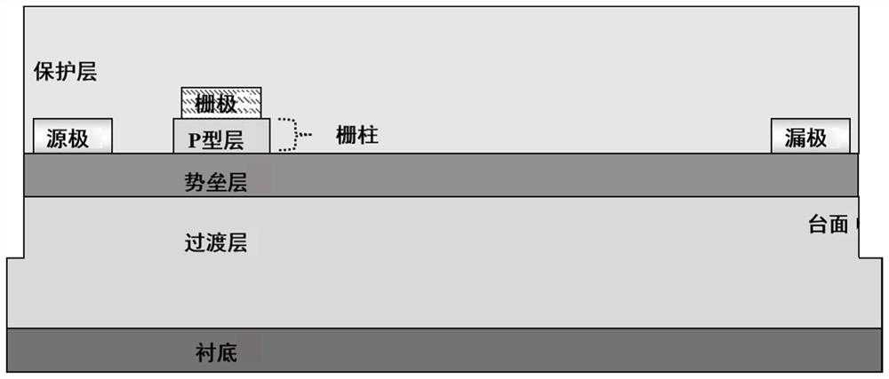
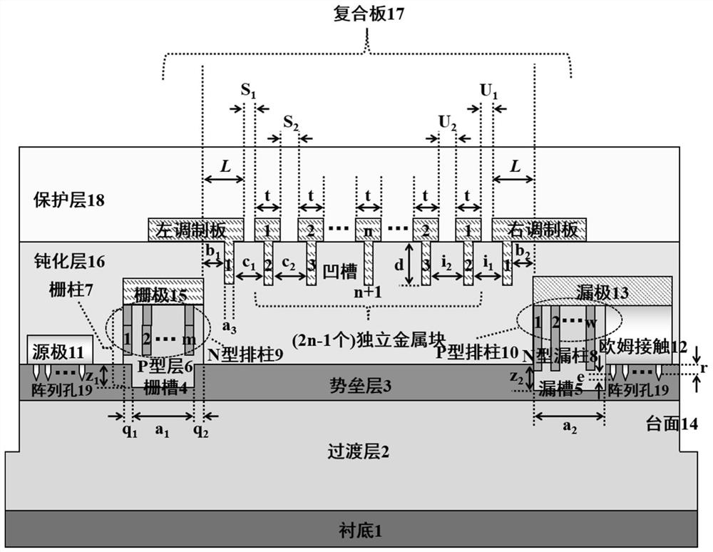
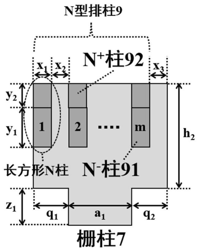
[0104] Embodiment 1: Making the thickness h of the P-type layer 6 above the barrier layer 3 2 20nm, the doping concentration of P-type layer 6 is 5×10 20 cm -3 , the length of gate column 7 is 4nm, and the doping concentration of N-type drain column 8 is 5×10 20 cm -3 , which lies at a thickness h above the barrier layer 3 1 is 10nm, and the depth of the P-type column 10 is u 1 7nm, doping concentration is 5×10 20 cm -3 , the number w of rectangular P columns is 1, N - column 91 depth y 1 10nm, doping concentration is 1×10 18 cm -3 , N + Depth y of column 92 2 8nm, doping concentration is 5×10 20 cm -3 , the number m of rectangular N columns is 1, the array hole 19 is composed of 2×2 holes of the same size, the number of grooves is 3, and the number of independent metal blocks is 1 junction gate-drain power device.

[0105] Step 1. Epitaxial GaN material is made transition layer 2 on sapphire substrate 1, as Figure 8 a.

[0106] 1a) GaN material with a thickne...

Embodiment 2

[0155] Embodiment 2: Making the thickness h of the P-type layer 6 above the barrier layer 3 2 200nm, the doping concentration of P-type layer 6 is 1×10 19 cm -3 , the length of gate column 7 is 1800nm, and the doping concentration of N-type drain column 8 is 5×10 19 cm -3 , which lies at a thickness h above the barrier layer 3 1 is 200nm, and the depth of the P-type column 10 is u 1 80nm, doping concentration is 1×10 19 cm -3 , the number w of rectangular P columns is 3, N - column 91 depth y 1 100nm, doping concentration 1×10 17 cm -3 , N + Depth y of column 92 2 80nm, doping concentration is 5×10 19 cm -3 , the number m of rectangular N pillars is 3, the array hole 19 is composed of 5×5 holes of the same size, the number of grooves is 5, and the number of independent metal blocks is 3 junction gate-drain power devices.

[0156] Step 1. Epitaxially AlN and GaN materials on the silicon carbide substrate 1 to form the transition layer 2, such as Figure 8 a.

[...

Embodiment 3

[0192] Embodiment 3: Making the thickness h of the P-type layer 6 above the barrier layer 3 2 400nm, the doping concentration of P-type layer 6 is 5×10 16 cm -3 , the length of gate column 7 is 5000nm, and the doping concentration of N-type drain column 8 is 1×10 16 cm -3 , which lies at a thickness h above the barrier layer 3 1 is 600nm, and the depth of the P-type column 10 is u 1 550nm, doping concentration is 1×10 16 cm -3 , the number w of rectangular P columns is 5, N - column 91 depth y 1 50nm, doping concentration is 1×10 11 cm -3 , N + Depth y of column 92 2 300nm, doping concentration is 1×1018 cm -3 , the number m of rectangular N pillars is 5, the array hole 19 is composed of 10×10 holes of the same size, the number of grooves is 7, and the number of independent metal blocks is 5 junction gate-drain power devices.

[0193] Step A. Epitaxial AlN and GaN materials on the silicon substrate 1 from bottom to top to make the transition layer 2, such as Fig...


PUM

PropertyMeasurementUnit
lengthaaaaaaaaaa
thicknessaaaaaaaaaa
electron work functionaaaaaaaaaa

Abstract

The invention discloses a junction gate-drain power device, which mainly solves the problems of low threshold voltage and complex process for realizing high breakdown voltage in existing power switching devices, which comprises: a substrate (1), a transition layer (2 ), barrier layer (3), gate groove (4), drain groove (5), P-type layer (6), gate column (7), N-type drain column (8), source electrode (11), ohmic contact (12), mesa (14), gate (15) and passivation layer (16). The inside of the N-type leakage column is provided with a P-type row column (81); There are array holes (10); a drain (13) is arranged above the N-type drain column and the ohmic contact; a composite board (17) is arranged on the upper part of the passivation layer; a protective layer (18) is arranged on the periphery of the passivation layer and the composite board ). The invention has the advantages of simple process, good forward blocking and reverse blocking, high threshold voltage, and can be used as a switching device.

Description

technical field [0001] The invention belongs to the technical field of microelectronics, in particular to a power switching device, which can be used as a basic device of a power electronic system. [0002] technical background [0003] Power electronic systems are widely used in many fields such as aerospace, industrial equipment, electric vehicles, and household appliances. As an important component of power electronic systems, power switching devices are important tools for energy conversion and control. Therefore, the performance and reliability of power switching devices have a decisive impact on the technical indicators and performance of the entire power electronic system. At present, the performance of Si-based power switching devices has approached its theoretical limit, which cannot meet the requirements of high temperature, high voltage, high frequency, high efficiency and high power density of the next generation power electronic system. The third-generation wide...

Claims


Application Information

Patent Timeline
Patent Type & Authority Patents(China)
IPC IPC(8): H01L29/423H01L29/40H01L29/06H01L29/778H01L21/335
CPCH01L29/0611H01L29/402H01L29/42316H01L29/66462H01L29/778
Inventor 毛维高北鸾杨翠马佩军张金风郑雪峰王冲张进成马晓华郝跃
Owner XIDIAN UNIV
Why Eureka
Try Eureka