
Multi-electron beam focusing apparatus and control method

A focusing device and electron beam technology, applied to circuits, discharge tubes, electrical components, etc., can solve problems such as limited improvement space, and achieve the effects of facilitating precise control, improving resolution, improving accuracy and speed

Pending Publication Date: 2020-11-03
深圳市奥谱太赫兹技术研究院
View PDF0 Cites 0 Cited by
  • Summary
  • Abstract
  • Description
  • Claims
  • Application Information

AI Technical Summary

Problems solved by technology

However, with this scheme, the number of electron beams depends entirely on the size of a single module. The size of a single module found in the current literature is 2 cm * 2 cm, so that only 16 electron beams can be accommodated on a 4-inch wafer.
Increasing the electron beam can only reduce the size of a single module, but it is foreseeable that there is limited room for improvement with this technology route

Method used


Image

  • Multi-electron beam focusing apparatus and control method
  • Multi-electron beam focusing apparatus and control method
  • Multi-electron beam focusing apparatus and control method

Examples


Embodiment Construction

[0043] The preferred embodiments of the present invention will be described below in conjunction with the accompanying drawings. It should be understood that the preferred embodiments described here are only used to illustrate and explain the present invention, and are not intended to limit the present invention.

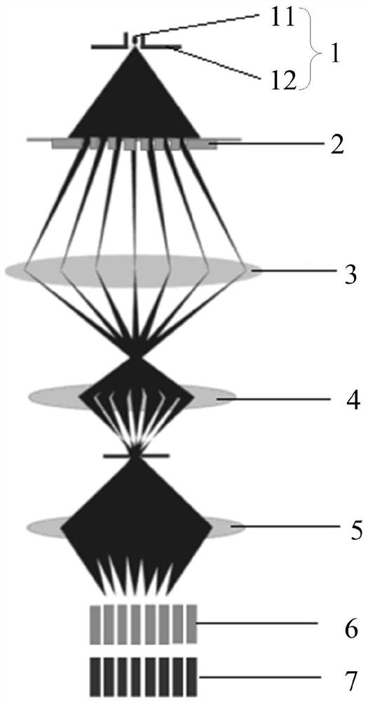
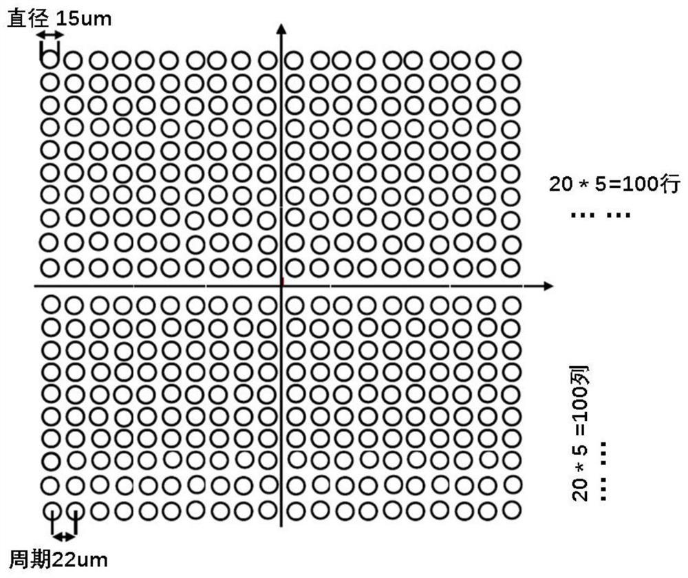
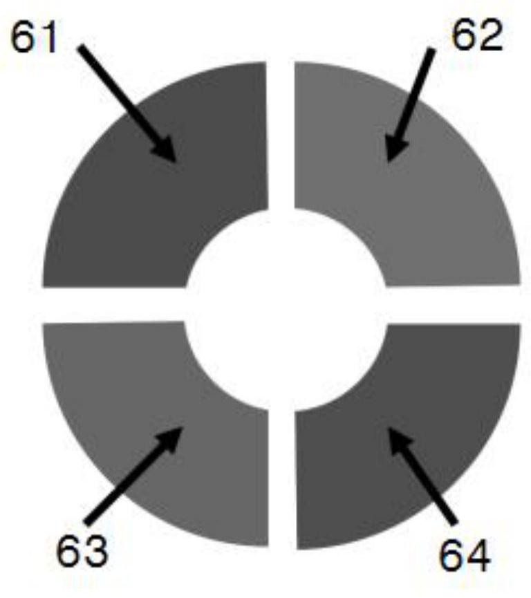
[0044] Please refer to Figure 1-8 As shown, the present invention provides a multi-electron beam focusing device, the system includes an electron beam emission source 1 for generating electron beams, a beam splitter 2 for splitting electron beams, an accelerating lens 3 for increasing the energy of electron beams, and increasing the electron beam energy. Dephasing lens 4 for beam quality, high-resolution objective lens array 5 for each electron beam spot, electron beam deflector 6 for fine-tuning electron beam position, and beam gate 7 for controlling electron beam passing, beam gate 7 and electron beam deflection The controller 6 is connected with a control circui...


PUM


Abstract

The invention discloses a multi-electron beam focusing device and a control method. The multi-electron-beam focusing device comprises a hot or cold field emission cathode electron source and a grid for generating electron beams, a beam splitter for splitting the electron beams, an accelerating lens for improving the energy of the electron beams, a phase difference eliminating lens for improving the quality of the electron beams, a high-resolution objective lens array for beam spots of the electron beams, an electron beam deflector used for finely adjusting the position of the electron beam, and a beam gate used for controlling the electron beam to pass through, so that the electron beam can be accurately controlled, more electron beams can be accommodated on wafers with the same area to realize simultaneous exposure, and the precision and the speed in integrated circuit processing application are improved.

Description

technical field [0001] The invention relates to the field of high-precision semiconductor processing, in particular to a multi-electron beam focusing device and a control method. Background technique [0002] Integrated circuit performance, such as computing speed and storage density, has followed Moore's Law in the past. In the past few decades, it has become faster and stronger, which has also driven the continuous development of chip processing technology and the development of higher-resolution processing technology. Until now, high-yield and high-precision patterning processing equipment has always been the core equipment of the semiconductor industry. At present, advanced chip processing requires 30 to 50 exposure processes, and the cost of the entire exposure process accounts for about 1 / 3 of the integrated circuit processing cost. Since the lithography machine can meet the needs of industrial production, it has developed into the only choice for exposure equipment i...

Claims


Application Information

Patent Timeline
Patent Type & Authority Applications(China)
IPC IPC(8): H01J37/317H01J37/30H01J37/21
CPCH01J37/3177H01J37/3007H01J37/21
Inventor 尹华碧
Owner 深圳市奥谱太赫兹技术研究院
Learn More