Packaging structure of silicon carbide Vienna rectifier half-bridge module

A packaging structure, silicon carbide technology, applied in the output power conversion device, conversion equipment structural parts, electric solid devices and other directions, can solve the problem of limiting the switching speed of power modules, high-frequency applications, large peak voltage of switching tube chips, limiting Converter operating frequency and other issues to achieve the effect of reducing coupling, reducing common source inductance, and reducing influence

Active Publication Date: 2020-11-10
HUAZHONG UNIV OF SCI & TECH
View PDF5 Cites 4 Cited by
  • Summary
  • Abstract
  • Description
  • Claims
  • Application Information

AI Technical Summary

Problems solved by technology

[0003] Theoretically, the switching frequency of silicon carbide devices can reach up to megahertz. However, most of the existing commercial devices have large parasitic inductance parameters, which makes the switch tube chip withstand a large peak voltage when it is turned off at high speed. The transient state produces a large oscillation, which brings greater loss, and may even break down the device
These effects will be more obvious at faster switching speed and higher switching frequency, which limits the improvement of power module switching speed and high frequency application
[0004] At present, there are power modules that realize bidirectional switching, but in practical applications (such as Vienna rectifiers), simple bidirectional switching power modules often need to be connected with other power devices, so large parasitic inductance will still be generated in the commutation circuit , thus limiting the operating frequency of the converter

Method used


Image

  • Packaging structure of silicon carbide Vienna rectifier half-bridge module
  • Packaging structure of silicon carbide Vienna rectifier half-bridge module
  • Packaging structure of silicon carbide Vienna rectifier half-bridge module

Examples


Embodiment Construction

[0031] In order to make the object, technical solution and advantages of the present invention clearer, the present invention will be further described in detail below in conjunction with the accompanying drawings and embodiments. It should be understood that the specific embodiments described here are only used to explain the present invention, not to limit the present invention. It is worth noting that the words indicating orientation or positional relationship, such as "upper", "lower", "left", "right", "middle", etc., are all based on the orientation or positional relationship shown in the drawings, and are only for description present invention, rather than limitation of the present invention. In addition, the technical features involved in the various embodiments of the present invention described below can be combined with each other as long as they do not constitute a conflict with each other.

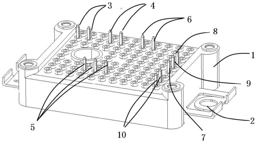
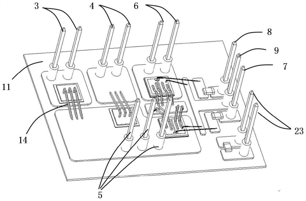
[0032] To achieve the above object, an embodiment of the present inventio...


PUM


Abstract

The invention discloses a packaging structure of a silicon carbide Vienna rectifier half-bridge module, and belongs to the technical field of power semiconductor devices. The packaging structure comprises a power unit and an insulating substrate. The power unit comprises a diode rectification upper bridge arm, a diode rectification lower bridge arm and a bidirectional switch bridge arm. The bidirectional switch bridge arm comprises a first silicon carbide MOSFET chip and a second silicon carbide MOSFET chip which share a common source and are connected in series. The surface copper layer of the insulating substrate comprises a positive electrode metal layer, a negative electrode metal layer, an input metal layer, an output metal layer, a bidirectional switch power common source electrode metal layer, a driving metal layer and a thermistor metal layer. The diode rectification upper bridge arm is located on the positive electrode metal layer, the diode rectification lower bridge arm andthe first silicon carbide MOSFET chip are located on the input metal layer, and the second silicon carbide MOSFET chip is located on the output metal layer. According to the present invention, the parasitic inductance in a current conversion loop is reduced, so that switching loss is reduced, and the packaging structure is more suitable for high-frequency application; and the power switch tube chip is driven by adopting Kelvin connection, so that the driving stability is enhanced.

Description

technical field [0001] The invention belongs to the technical field of power semiconductor devices, and more specifically relates to a packaging structure of a silicon carbide Vienna rectifier half-bridge module. Background technique [0002] Compared with traditional silicon-based power devices, silicon carbide power devices have higher breakdown voltage, smaller volume, higher thermal conductivity and higher operating temperature, so they are more suitable for high voltage, high temperature and high frequency applications. scene. In order to pursue a smaller converter size, the switching frequency of the power supply system continues to increase, the switching speed of the switching tube in the power module continues to increase, and the switching loss continues to decrease. In the high-frequency field, silicon carbide devices have great prospects. [0003] Theoretically, the switching frequency of silicon carbide devices can reach up to megahertz. However, most of the e...

Claims


Application Information

Patent Timeline
Patent Type & Authority Applications(China)
IPC IPC(8): H01L25/16H01L29/78H01L29/872H01L29/16H01L23/498H02M7/00H02M7/12H02M7/219
CPCH01L25/16H01L29/78H01L29/872H01L29/1608H01L23/49838H02M7/003H02M7/125H02M7/219H01L2224/48227H01L2224/49111Y02B70/10
Inventor 彭力花伟杰陈材黄志召刘新民康勇
Owner HUAZHONG UNIV OF SCI & TECH
Why Eureka
Try Eureka