A kind of insulated gate bipolar transistor and its forming method

A bipolar transistor, insulated gate technology, applied in the manufacture of transistors, semiconductor devices, semiconductor/solid-state devices, etc., can solve the problem of difficulty in preparing hydrogen-doped regions with stable distribution, and achieve the effect of smooth voltage changes and improved performance

Active Publication Date: 2021-01-29
SEMICON MFG ELECTRONICS (SHAOXING) CORP
View PDF1 Cites 1 Cited by
  • Summary
  • Abstract
  • Description
  • Claims
  • Application Information

AI Technical Summary

Problems solved by technology

[0004] The purpose of the present invention is to provide a method for forming an insulated gate bipolar transistor, so as to solve the difficulty in preparing a hydrogen-doped region with stable distribution in the existing forming method, which is conducive to improving the performance stability of the formed transistor device

Method used


Image

  • A kind of insulated gate bipolar transistor and its forming method
  • A kind of insulated gate bipolar transistor and its forming method
  • A kind of insulated gate bipolar transistor and its forming method

Examples


Embodiment Construction
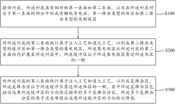
[0054] The core idea of ​​the present invention is to provide a method for forming an insulated gate bipolar transistor, which is conducive to improving the preparation accuracy of the buffer layer in the device.

[0055] specific reference figure 1 As shown, the forming method of the insulated gate bipolar transistor may include:

[0056] Step S100, providing a substrate, the substrate has an opposite first surface and a second surface, and a gate conductive layer, a body of the first doping type are formed in a part of the substrate corresponding to the first surface region and an emitter region of a second doping type;

[0057] Step S200, performing an ion implantation process and an annealing process on the second surface of the substrate to form a buffer region of the second doping type and a collector region of the first doping type;

[0058] Step S300, performing an ion implantation process on the second surface of the substrate to form a hydrogen-doped hydrogen-doped...


PUM


Abstract

The present invention provides an insulation grid bipolar transistor and its formation method.In this formation method, after forming a first -doping type of collector region and a second doped buffer, a hydrogen doping is formed, which can avoidThe impact of the processing process is conducive to improving the control process of the preparation process in the hydrogen doping area, and it is easier to form multiple hydrogen doping regions that reduce the peak of the ion concentration on the surface of the substrate surface in order.At this time, a hydrogen doped area that can be accurately controlled based on the buffer and concentration distribution based on the formed can enable the transistor device to achieve high -efficiency electric field cuts and improve the performance of the transistor device.

Description

technical field [0001] The invention relates to the technical field of semiconductors, in particular to an insulated gate bipolar transistor and a forming method thereof. Background technique [0002] Insulated Gate Bipolar Transistor (IGBT, Insulated Gate Bipolar Transistor), which combines the gate voltage control characteristics of MOSFET and the low on-resistance characteristics of bipolar transistors, improves the mutual restraint of device withstand voltage and on-resistance , has the advantages of high voltage, high current, high frequency, high power integration density, large input impedance, small on-resistance, and low switching loss. It has gained wide application space in many fields such as frequency conversion home appliances, industrial control, electric and hybrid vehicles, new energy, and smart grid. [0003] Generally speaking, as the substrate thickness of the IGBT (that is, the thickness of the drift region) increases, the turn-off voltage of the device...

Claims


Application Information

Patent Timeline
Patent Type & Authority Patents(China)
IPC IPC(8): H01L29/739H01L29/06H01L21/331
CPCH01L29/7393H01L29/0603H01L29/0684H01L29/66333
Inventor 王珏陈政戴银徐杨徐承福
Owner SEMICON MFG ELECTRONICS (SHAOXING) CORP
Why Eureka
Try Eureka