
Multi-state memory, preparation method and storage method thereof and artificial synaptic device

A memory and polygon technology, applied in static memory, digital memory information, information storage, etc., can solve the problems of polymorphic storage instability, unfavorable practical application, and broken symmetry, and achieve fast reading speed, low power consumption, The effect of increasing storage density

Active Publication Date: 2020-11-13
LANZHOU UNIVERSITY
View PDF13 Cites 1 Cited by
  • Summary
  • Abstract
  • Description
  • Claims
  • Application Information

AI Technical Summary

Problems solved by technology

For a single antiferromagnetism, although the multistate storage function can be realized, and the storage state is very stable, but because the antiferromagnetism does not appear magnetic to the outside, the current signal reading of the multistate storage based on antiferromagnetism mainly depends on Anisotropic magnetoresistance, which is a weak signal for practical applications
The multi-state storage based on ferromagnetic materials uses the characteristic that changes in ferromagnetic domains will cause resistance changes to realize multi-state storage. Since the external magnetic field will affect the movement of ferromagnetic domains, such multi-state storage is unstable.
In addition, the existing methods of using spin current to drive magnetization reversal or magnetic domain movement require an auxiliary magnetic field to break the symmetry in order to realize the magnetic moment reversal under current drive, which is not conducive to the practical application of this effect.

Method used


Image

  • Multi-state memory, preparation method and storage method thereof and artificial synaptic device
  • Multi-state memory, preparation method and storage method thereof and artificial synaptic device

Examples


Embodiment Construction

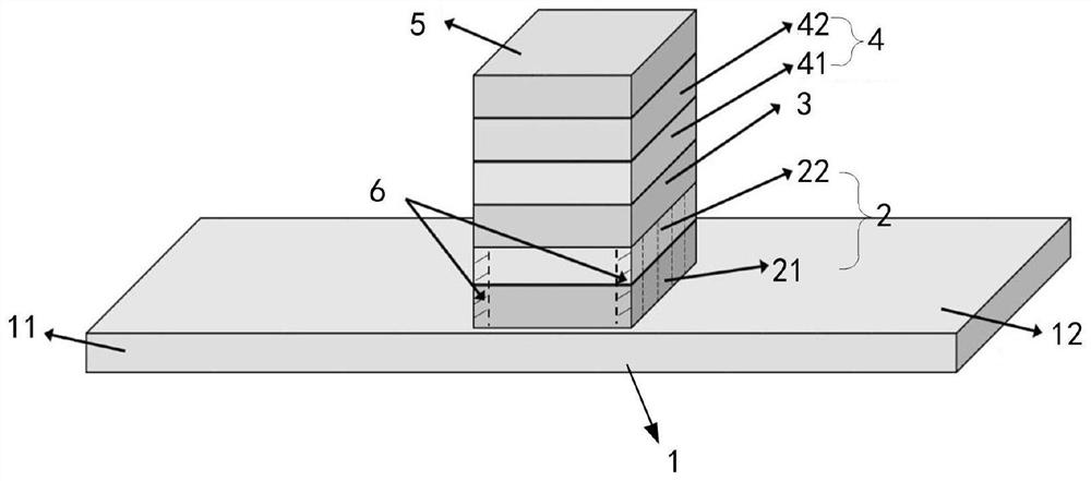
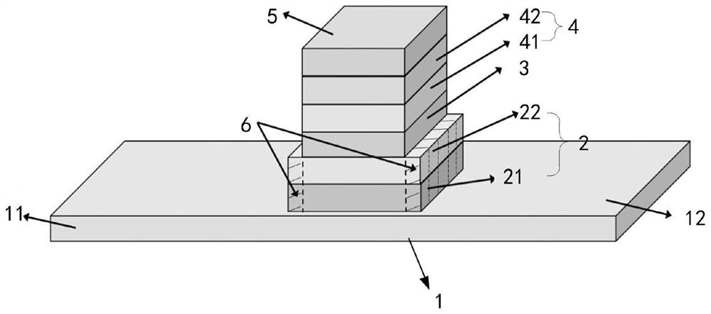
[0047] In order to further explain the technical means and effects of the present invention to achieve the intended purpose of the invention, the following describes a multi-state memory according to the present invention, its preparation method, storage method and artificial burst memory in conjunction with the accompanying drawings and preferred embodiments. The specific implementation of the contactor and its effect are described in detail below.

[0048] An embodiment of the present invention provides a multi-state memory, such as figure 1 with figure 2 As shown, the multi-state memory is a multi-state memory based on two exchange bias layers, and has a multi-layer thin film structure, including: spin current generation layer 1, first exchange bias layer 2, insulating material layer from bottom to top 3. The second exchange bias layer 4 and the upper electrode 5 .

[0049] Wherein, the first exchange bias layer 2 includes a lower antiferromagnetic layer 21 and a lower f...


PUM


Abstract

The invention discloses a multi-state memory, a preparation method and a storage method thereof and an artificial synaptic device. The multi-state memory is provided with a multi-layer thin film structure and sequentially comprises a spin current generation layer, a first exchange bias layer, an insulating material layer, a second exchange bias layer and an upper electrode from bottom to top, wherein the spin current generation layer is used for generating a spin current for applying a spin orbital moment to a magnetic moment; the first exchange bias layer is used for storing data; the insulating material layer is used for providing vertical magnetic anisotropy; the second exchange bias layer is used for reading the tunneling magnetoresistance; a first electrode and a second electrode arearranged at the two ends of the spin current generation layer respectively, and a write current is applied between the first electrode and the second electrode to store data; and a read current is applied between the second electrode and the upper electrode to read data. The storage density and the storage stability of the multi-state memory are effectively improved, the storage power consumptionis reduced, and the anti-interference capability of the memory is improved.

Description

technical field [0001] The invention relates to information storage and semiconductor fields, in particular to a multi-state memory based on two exchange bias layers composed of antiferromagnetic and ferromagnetic materials, its preparation method, multi-state storage method and artificial synapse. Background technique [0002] With the rapid development of the information age, the era of big data has come, which requires increasing the data storage density of the current memory, so polymorphic storage has been widely studied. Compared with traditional computer binary storage, polymorphic storage realizes the storage of multiple bytes in one storage unit, which can greatly increase the information storage density. On the other hand, although the computer based on the "von Neumann" configuration shows great advantages in data calculation, it is far behind the human brain in terms of image recognition and learning ability; Under the circumstances, the power consumption of the...

Claims


Application Information

Patent Timeline
IPC IPC(8): H01L43/08H01L43/12G11C11/16
CPCG11C11/161H10N50/01H10N50/10Y02D10/00
Inventor 席力貟吉军常美霞左亚路杨德政薛德胜
Owner LANZHOU UNIVERSITY
Learn More