Spliced graphite bipolar plate of vanadium battery
A bipolar plate and vanadium battery technology, applied in the field of vanadium batteries, can solve the problems of increasing the amount of conductive bipolar plates, reducing the energy efficiency of the stack, and increasing the cost of materials, so as to reduce the internal leakage current of the battery, accelerate the crystallization speed, and improve the The effect of the service life
- Summary
- Abstract
- Description
- Claims
- Application Information
AI Technical Summary
Problems solved by technology
Method used
Image
Examples
Embodiment 1
[0026] A vanadium battery spliced graphite bipolar plate, the preparation process of which is as follows:
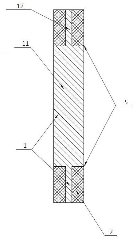
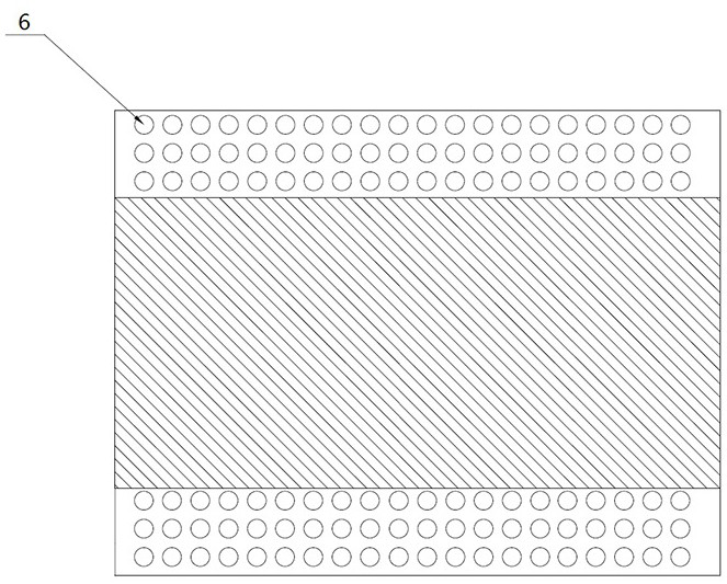
[0027] Preparation of conductive plate 1: Put the expanded graphite and conductive graphite powder into the mold according to the ratio of 90:10, apply a pressure of 30 MPa, hold the pressure for 15 min, prepare the conductive plate substrate, and place the conductive plate substrate on the engraving machine. , the protruding strip structure 12 of the conductive plate 1 is processed and punched with round holes, the diameter of which is 1 mm, and the round holes are evenly arranged. The thickness of the square plate-shaped structure 11 of the conductive plate 1 is 1 mm, and the thickness of the protruding strip-shaped structure 12 is 0.4 mm.
[0028] Preparation of non-conductive plate 2: Mass fraction of non-conductive plate 2 components: polypropylene PP 70%, silicon dioxide 30%. The above raw materials are weighed and uniformly mixed at a high speed in a high-speed...
Embodiment 2
[0031] A vanadium battery spliced graphite bipolar plate, the preparation process of which is as follows:
[0032] Preparation of conductive plate 1: Put the expanded graphite and conductive graphite powder into the mold according to the ratio of 92:8, apply a pressure of 40 MPa, hold the pressure for 10 min, prepare the conductive plate substrate, and place the conductive plate substrate on the engraving machine. , the protruding strip structure 12 of the conductive plate 1 is processed and punched with circular holes, the diameter of which is 1.5 mm, and the circular holes are evenly arranged. The thickness of the square plate-shaped structure 11 of the conductive plate 1 is 2 mm, and the thickness of the protruding strip-shaped structure 12 is both 0.8 mm.
[0033] Preparation of non-conductive plate 2: The mass fraction of non-conductive plate 2 components: polyethylene PE 80%, titanium dioxide 20%. The above raw materials are weighed and uniformly mixed at a high speed...
Embodiment 3
[0036] A vanadium battery spliced graphite bipolar plate, the preparation process of which is as follows:
[0037] Preparation of conductive plate 1: Put the expanded graphite and conductive graphite powder into the mold according to the ratio of 95:5, apply a pressure of 40 MPa, maintain the pressure for 10 min, prepare the conductive plate substrate, and place the conductive plate substrate on the engraving machine. , the protruding strip structure 12 of the conductive plate 1 is processed and punched with circular holes, the diameter of which is 2.0 mm, and the circular holes are evenly arranged. The thickness of the square plate-like structure 11 of the conductive plate 1 is 3 mm, and the thickness of the protruding strip-like structure 12 is both 1.2 mm.
[0038] Preparation of non-conductive plate 2: The mass fraction components of non-conductive plate 2: epoxy resin 70%, titanium dioxide 20%, silicate 10%. The above raw materials are weighed and then mixed in an inte...
PUM
| Property | Measurement | Unit |
|---|---|---|
| Particle size | aaaaa | aaaaa |
| Thickness | aaaaa | aaaaa |
| Thickness | aaaaa | aaaaa |
Abstract
Description
Claims
Application Information


