Ultraviolet, visible and infrared wide-spectrum photoelectric detector and preparation method thereof
A photodetector and infrared technology, applied in the field of detectors, can solve the problems of complex preparation process and high preparation cost, and achieve the effects of improving light absorption and light response, large aspect ratio and low cost
- Summary
- Abstract
- Description
- Claims
- Application Information
AI Technical Summary
Problems solved by technology
Method used
Image
Examples
Embodiment 1
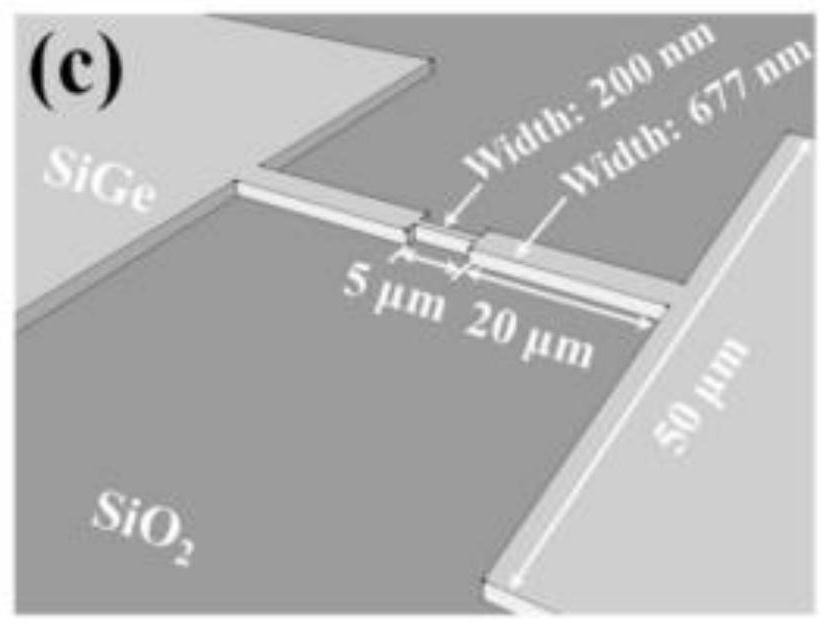
[0055] The Ge heterojunction nanowire structure proposed in the article "Broadband 400-2400nm Ge heterostructure nanowire photodetector fabricated by three-dimensional Ge condensation technique" published by Lin Guangning and others in 2019 can achieve detection in the range of 400-2400nm. The preparation process is as follows: First, 5nm Si and 99nm Si are grown on a silicon-on-insulator (SOI) substrate 0.76 Ge 0.24 layer, at 1150°C, 95nm Si will be formed in the buried oxide layer 0.67 Ge 0.3 layer. Then buffered oxide etchant (BOE, Buffered OxideEtch) was used to remove the surface SiO generated during planar Ge condensation. 2 , to determine the pattern formed on the SiGe layer. By electron beam lithography (EBL, E-Beam Lithography) and reactive ion etching (RIE, Reactive ion etching) technology, insulator nanowires were prepared along the [110] orientation on the buried oxide layer. For the pattern, please refer to figure 1 , figure 1 It is a structural schematic di...
Embodiment 2
[0105] see again Figure 4 , this embodiment also provides an ultraviolet, visible and infrared wide-spectrum photodetector on the basis of the above-mentioned embodiment, the ultraviolet, visible and infrared wide-spectrum photodetector is prepared by the preparation method of the above-mentioned embodiment, the photoelectric Detectors include:
[0106] Metal film 50, the material of metal film 50 is Au;
[0107] a glass substrate 10 located on the metal film 50;
[0108] The electrode array 20 is located on the glass substrate 10. The electrode array 20 includes a number of metal electrodes arranged at intervals. The material of the metal electrodes is, for example, Au;
[0109] The ZnO nanowire film 30 is located on the electrode array 20 and the glass substrate 10, and the ZnO nanowire film 30 covers the electrode array 20;
[0110] The Ge quantum dot film 40 is located on the ZnO nanowire film 20 .
[0111] In the description of the present invention, the terms "first...
PUM
 Abstract
Description
Claims
Application Information


