Preparation method of rare earth doped indium sulfide nanosheet film photoanode and product thereof

A rare earth doping, photoanode technology, applied in chemical instruments and methods, electrodes, electrolysis processes, etc., to achieve high energy transfer efficiency, inhibit recombination, and improve photoelectrochemical performance.

Active Publication Date: 2020-11-27
NORTHWEST UNIV
View PDF5 Cites 1 Cited by
  • Summary
  • Abstract
  • Description
  • Claims
  • Application Information

AI Technical Summary

Problems solved by technology

Different from transition metal ions, trivalent lanthanide rare earth ions have rich energy level structures and excellent optical properties, which have recently attracted the attention of researchers. There...

Method used


Image

  • Preparation method of rare earth doped indium sulfide nanosheet film photoanode and product thereof
  • Preparation method of rare earth doped indium sulfide nanosheet film photoanode and product thereof
  • Preparation method of rare earth doped indium sulfide nanosheet film photoanode and product thereof

Examples


Embodiment 1

[0025] This example prepares β-In 2 S 3 :Yb 3+ -Tm 3+ Thin film photoelectrode material, In 3+ :Yb 3+ :Tm 3+ =197:2:1

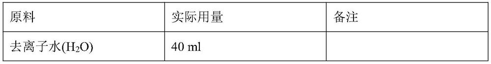
[0026] The raw materials used are shown in Table 1:

[0027] Table 1

[0028]

[0029]

[0030] Preparation:

[0031] 1) First, clean the FTO glass, place the FTO glass in deionized water, ethanol, and acetone for 30 minutes of ultrasonic treatment and blow dry for later use.

[0032] 2) Weigh indium chloride, thioacetamide, ytterbium nitrate, thulium nitrate, and 40ml of deionized water, transfer to a beaker and stir for 30 minutes, in which indium chloride, thioacetamide, ytterbium nitrate, and thulium nitrate Quantities are 0.9456mmol, 2.88mmol, 0.0096mmol, 0.0048mmol, guaranteed In 3+ :Yb 3+ :Tm 3+ =197:2:1, S 2- The amount of the substance is 3 times the sum of the amount of all cationic substances, the concentration of indium chloride, ytterbium nitrate, and thulium nitrate is 24mM, and the concentration of thioacetamide is 72mM.

[...

Embodiment 2

[0035] This example prepares β-In 2 S 3 :Yb 3+ -Tm 3+ Thin film photoelectrode material, In 3+ :Yb 3+ :Tm 3+=193:6:1

[0036] The raw materials used are shown in Table 2;

[0037] Table 2

[0038]

[0039] Preparation:

[0040] 1) First, clean the FTO glass, place the FTO glass in deionized water, ethanol, and acetone for 30 minutes of ultrasonic treatment and blow dry for later use.

[0041] 2) Weigh indium chloride, thioacetamide, ytterbium nitrate, thulium nitrate, and 40ml of deionized water, transfer to a beaker and stir for 30 minutes, in which indium chloride, thioacetamide, ytterbium nitrate, and thulium nitrate Quantities are 0.9264mmol, 2.88mmol, 0.0288mmol, 0.0048mmol, guaranteed In 3+ :Yb 3+ :Tm 3+ =193:6:1, S 2- The amount of the substance is 3 times the sum of the amount of all cationic substances, the concentration of indium chloride, ytterbium nitrate, and thulium nitrate is 24mM, and the concentration of thioacetamide is 72mM.

[0042] Transfe...

Embodiment 3

[0044] This example prepares β-In 2 S 3 :Yb 3+ -Tm 3+ Thin film photoelectrode material, In 3+ :Yb 3+ :Tm 3+ =189:10:1

[0045] The raw materials used are shown in Table 3;

[0046] table 3

[0047]

[0048] Preparation:

[0049] With embodiment 1, difference is, preparation raw material indium chloride (InCl 3 4H 2 O), ytterbium nitrate (Yb(NO 3 ) 3 ·6H 2 O), thulium nitrate (Tm(NO 3 ) 3 ·6H 2 O) molar ratio In 3+ :Yb 3+ :Tm 3+ =189:10:1. Wherein indium chloride, thioacetamide, ytterbium nitrate, and thulium nitrate are respectively 0.9072mmol, 2.88mmol, 0.048mmol, and 0.0048mmol;

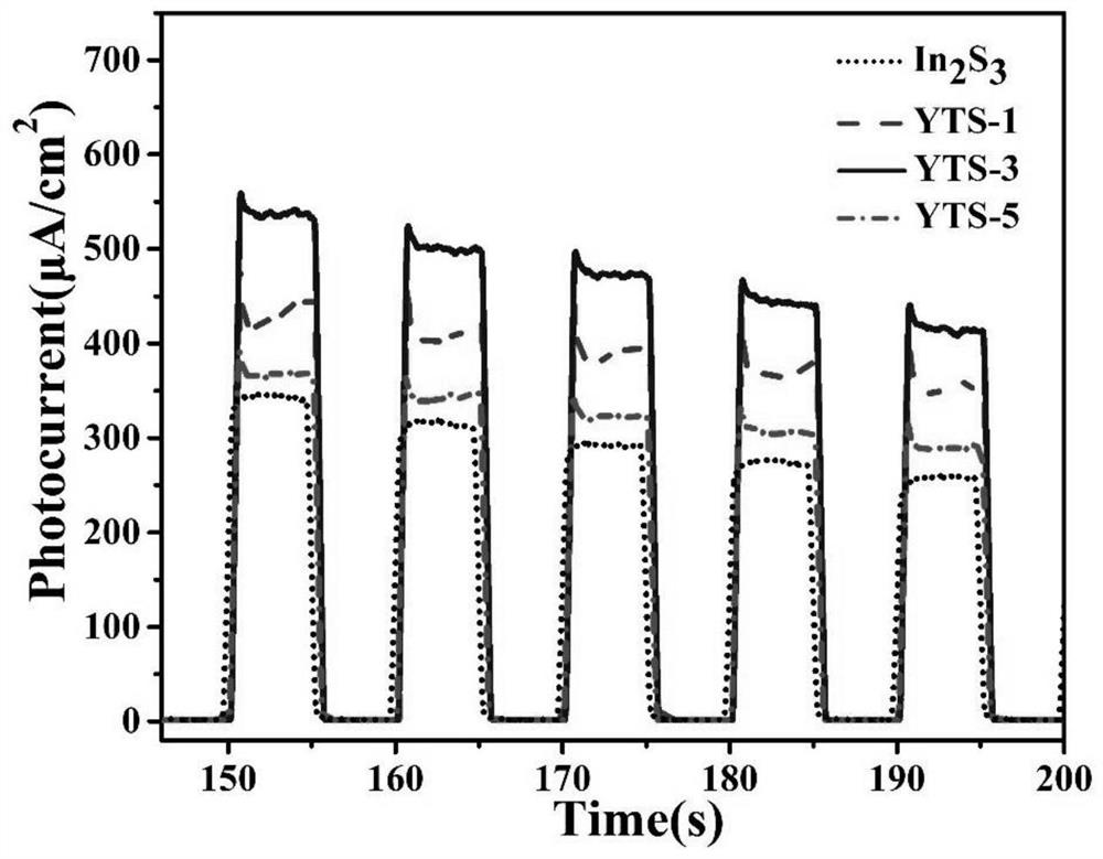
[0050] The prepared film (YTS-5) was taken out from the reactor, rinsed and dried with deionized water. The photocurrent density of the prepared thin film (YTS-5) reached 0.28mA / cm 2 , with pure β-In 2 S 3 Compared with the photoelectrochemical performance, it has a significant improvement, which is about pure β-In 2 S 3 (0.25mA / cm 2 ) 1.14 times ( figure 1 ).


PUM

PropertyMeasurementUnit
Photocurrent densityaaaaaaaaaa

Abstract

The invention discloses a preparation method of a rare earth doped indium sulfide nanosheet film photoanode and a product thereof. The preparation method comprises the following steps: dissolving thulium nitrate, ytterbium nitrate, an indium source and a sulfur source into water, stirring to obtain a precursor solution, putting the precursor solution into a reaction kettle, leaning conductive glass into the reaction kettle with the conductive surface facing downwards, keeping the temperature at 170-200 DEG C for 20-24 hours, taking out, and drying to obtain the rare earth doped indium sulfidenanosheet film photoanode. The thulium ions and ytterbium ions are doped in the indium sulfide nanosheet film, so that the photocurrent density and the photoelectrochemical performance of the indium sulfide nanosheet film photoanode are remarkably improved.

Description

technical field [0001] The invention relates to the technical field of photoelectric catalysis, in particular to a method for preparing a rare earth-doped indium sulfide nanosheet thin-film photoanode and a product thereof. Background technique [0002] Indium sulfide (In 2 S 3 ) has good narrow bandgap, high stability, low toxicity and other characteristics, as well as a variety of morphologies including nanosheets, nanotubes, nanorods and hollow microspheres, which makes it not only as a wide-spectrum photocatalytic / photoelectric It is a good candidate for catalyst and can be used as an excellent sensitizer for wide-bandgap photocatalysis / photoelectrocatalyst. However, In 2 S 3 The photocatalytic / photoelectrocatalytic efficiencies are still low due to the fast recombination of self-photogenerated carriers. Up to now, many methods have been used to improve the In 2 S 3 photocatalytic / photoelectrocatalytic efficiency, including the controlled synthesis of In 2 S 3 d...

Claims


Application Information

Patent Timeline
IPC IPC(8): C25B1/00C25B11/06B01J27/04B01J35/00B01J35/02
CPCB01J27/04B01J35/0033B01J35/004B01J35/023Y02P20/133
Inventor 胡晓云李秋洁苗慧樊君刘恩周成宇飞王佳伟张德恺赵俊峰
Owner NORTHWEST UNIV
Why Eureka
Try Eureka