
Perovskite solar cell with high fill factor and method for preparing perovskite solar cell

A solar cell and fill factor technology, which is applied to circuits, photovoltaic power generation, electrical components, etc., can solve problems such as the inability to prepare large-area solar cell devices, and achieve the effects of improving photoelectric conversion efficiency, meeting commercial use, and improving efficiency

Active Publication Date: 2019-02-19
XI AN JIAOTONG UNIV
View PDF5 Cites 14 Cited by
  • Summary
  • Abstract
  • Description
  • Claims
  • Application Information

AI Technical Summary

Problems solved by technology

To overcome the shortcomings of the existing spin-coating technology that cannot prepare large-area solar cell devices, use alkali metal halides or alkaline earth metal halides to prepare interface passivation layers to reduce carrier recombination at the interface between the perovskite light-absorbing layer and the electron transport layer , improve the efficiency of solar cells, and also enable mass production of large-area cells

Method used


Image

  • Perovskite solar cell with high fill factor and method for preparing perovskite solar cell
  • Perovskite solar cell with high fill factor and method for preparing perovskite solar cell
  • Perovskite solar cell with high fill factor and method for preparing perovskite solar cell

Examples


preparation example Construction

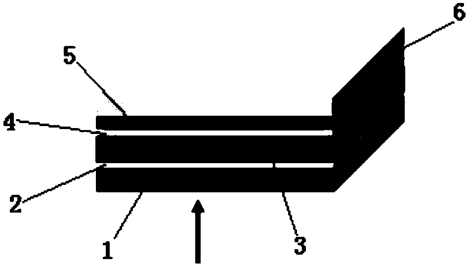
[0036] The present invention also provides a method for preparing the perovskite solar cell with the above-mentioned high fill factor, comprising the following steps:

[0037] In step S1, the transparent conductive substrate 1 is cleaned by three methods of ethanol cleaning, acetone ultrasonic cleaning and deionized water ultrasonic cleaning. dry to obtain a dry transparent conductive substrate 1.

[0038] Preferably, the transparent conductive substrate 1 is glass or a flexible substrate; wherein the flexible substrate is a polyimide compound or a polyesterimide compound.

[0039] Preferably, the conductive film is an inorganic conductive polymer or an organic conductive polymer; the inorganic conductive polymer is indium tin oxide, zinc oxide, tin oxide, gold, copper, silver or zinc; the organic conductive polymer is polythiophene, polyvinylbenzene sodium sulfonate or polyaniline.

[0040] Preferably, the sheet resistance of the conductive film is 15-30Ω, and its thickness...

Embodiment 1

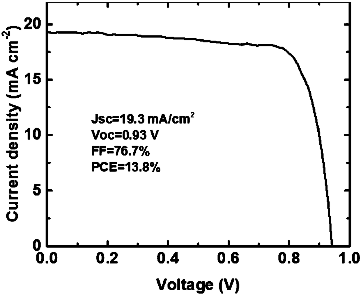
[0049] Preparation of perovskite solar cells, its structure is: transparent conductive substrate / ITO(130nm) / CH3NH3PbI3(400nm) / RbF(3nm) / C60(10nm) / BCP(6nm) / Ag(120nm); the specific process is as follows :

[0050] Step S1, cleaning the transparent conductive substrate pre-engraved with a conductive film, cleaning the transparent conductive substrate by sequentially performing ethanol cleaning, acetone ultrasonic cleaning and deionized water ultrasonic cleaning, and placing it under an infrared lamp after cleaning Drying, wherein the conductive thin film on the transparent conductive substrate is used as the anode layer of the solar cell, the square resistance of the conductive thin film is 15Ω, and the film thickness is 130nm. Wherein the transparent conductive substrate is glass, and the conductive film is indium tin oxide.

[0051] Step S2, treat the transparent conductive substrate processed in step S1 with ultraviolet ozone for 6 minutes; spin-coat the PH1000 solution on the...

Embodiment 2

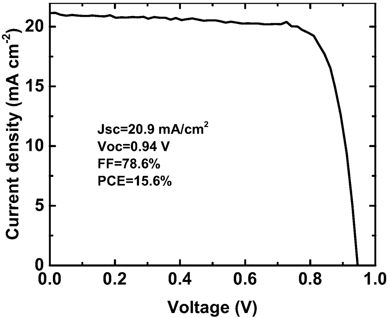
[0059] Preparation of perovskite solar cells, its structure is: transparent conductive substrate / ITO(120nm) / CH3NH3PbI3(400nm) / CsF(3nm) / PCBM(10nm) / BCP(6nm) / Au(100nm); the specific process is as follows :

[0060] Step S1, cleaning the transparent conductive substrate pre-engraved with a conductive film, cleaning the transparent conductive substrate by sequentially performing ethanol cleaning, acetone ultrasonic cleaning and deionized water ultrasonic cleaning, and placing it under an infrared lamp after cleaning Drying, wherein the conductive thin film on the transparent conductive substrate is used as the anode layer of the solar cell, the square resistance of the conductive thin film is 20Ω, and the film thickness is 120nm. Wherein the transparent conductive substrate is glass, and the conductive film is indium tin oxide.

[0061]Step S2, treat the transparent conductive substrate processed in step S1 with ultraviolet ozone for 6 minutes; spin-coat the PH1000 solution on the...


PUM

PropertyMeasurementUnit
Thicknessaaaaaaaaaa
Thicknessaaaaaaaaaa
Thicknessaaaaaaaaaa

Abstract

The invention discloses a perovskite solar cell with a high fill factor and a method for preparing the perovskite solar cell. The perovskite solar cell is sequentially provided with a transparent conductive substrate, a hole transport layer, a perovskite thin film, an interface passivation layer, an electron transport layer and a cathode from bottom to top. The interface passivation layer is madefrom alkali metal halide or alkaline earth metal halide on the perovskite thin film by means of evaporation, and the thickness of the interface passivation layer ranges from 1 nm to 5 nm; the electrontransport layer is a C<60> thin film formed on the interface passivation layer by means of evaporation, and the thickness of the C<60> thin film ranges from 10 nm to 20 nm; the cathode is a metal thin film formed on the electron transport layer by means of evaporation, and the thickness of the metal thin film ranges from 50 nm to 120 nm; the perovskite thin film is made from methylamine lead halide or formamidine lead halide; conductive thin films are arranged on the transparent conductive substrate. The perovskite solar cell and the method have the advantages that the shortcoming of incapability of preparing large-area solar cell devices by the aid of existing spin-coating technologies can be overcome by the aid of the perovskite solar cell and the method; the interface passivation layeris prepared by the aid of processes for carrying out evaporation on the alkali metal halide or the alkaline earth halide, accordingly, current carrier recombination at interfaces of perovskite lightabsorption layers and the electron transport layer can be reduced, the efficiency of the perovskite solar cell can be improved, and mass production of large-area cells further can be implemented.

Description

technical field [0001] The invention belongs to the technical field of perovskite solar cells; in particular, it relates to a perovskite solar cell with a high filling factor; it also relates to a preparation method of the solar cell. Background technique [0002] In recent years, organic lead halide perovskite materials have attracted great attention due to their ability to fabricate low-cost, high-efficiency solar cells. High solar cell efficiency benefits from the excellent photoelectric properties and unique defect properties of perovskite materials, which lead to low carrier recombination rates in perovskite materials. Inside the grains of perovskite materials, the diffusion length of carriers can exceed the light attenuation length of the material. At the same time, due to the development of the passivation process, the recombination of carriers at the grain boundaries can also be significantly reduced, which can further improve the efficiency of perovskite solar cell...

Claims


Application Information

Patent Timeline
IPC IPC(8): H01L51/42H01L51/48
CPCH10K71/311H10K30/353Y02E10/549Y02P70/50
Inventor 吴朝新牛永雷霆徐洁董化侯洵
Owner XI AN JIAOTONG UNIV
Learn More