Nanoscale field effect transistor based on MnBi2Te4 single layer
A field-effect transistor and nano-scale technology, which is applied in the field of nano-scale electronic devices, can solve the problems of few reports on the design of field-effect transistor devices, and achieve the effects of obvious field effect, excellent rectification performance and ultra-thin structure.
- Summary
- Abstract
- Description
- Claims
- Application Information
AI Technical Summary
Problems solved by technology
Method used
Image

Examples
Embodiment
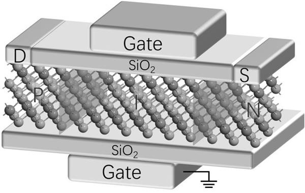
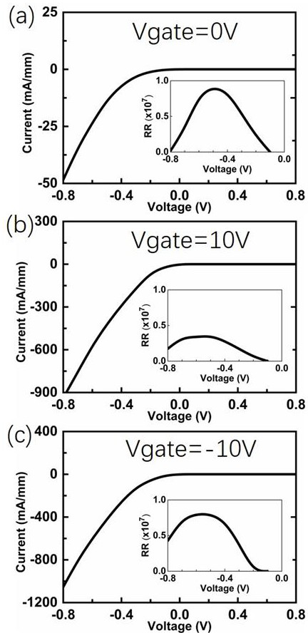
[0013] The present invention constructs by MnBi 2 Te 4 The single-layer structure of the material is P-type doped and N-type doped at both ends, while the middle region is retained as its intrinsic structure, and silicon dioxide dielectric and gate are applied on the upper and lower sides to obtain the PIN junction field effect transistor. The present invention uses industry's advanced device design tool QuantumATK ( Smidstrup, et al., QuantumATK: an integrated platform of electronic and atomic-scale modeling tools [J]. J. Phys.: Condens. Matter 32, 015901 (2020)) for device model design and performance measurement.
[0014] The MnBi-based 2 Te 4 The field effect properties of single-layer nanoscale PIN junction field effect transistors provide relevant theoretical basis and model construction schemes for the further design and realization of field effect transistor devices with ultra-thin structure, low power consumption, excellent performance and adjustable size.
[00...
PUM
 Abstract
Description
Claims
Application Information