Method for transferring solar cell substrate

A technology of solar cells and transfer methods, applied in the field of solar cells, can solve problems such as corrosion, influence on bonding quality, complexity, etc., and achieve the effects of reducing manufacturing costs, reducing battery costs, and improving service life

Inactive Publication Date: 2020-12-01
NANCHANG KAIXUN PHOTOELECTRIC CO LTD
View PDF6 Cites 4 Cited by
  • Summary
  • Abstract
  • Description
  • Claims
  • Application Information

AI Technical Summary

Problems solved by technology

[0019] In the technical step (3), there is a strong dependence on professional substrate stripping equipment. At present, there is no equipment suitable for industrial stripping. The stripping time is quite long, about 6 to 10 hours per piece; in addition, the stripping time is long. Susceptible to corrosion, which affects product yield and is not conducive to large-scale production;
[0020] In technical steps (4) and (6), the thinner epitaxial layer and flexible substrate are peeled off, and the structure is larger than 30-40 microns. The temporary bonding operation is more complicated, and the quality of bonding is extremely high; after bonding, a process is required. A series of device processing, because there is a layer of glue between the battery structure and the supporting substrate, the cleaning and etching in the process will corrode the bonding layer due to the solution, which will affect the quality of the bonding and cause delamination; in addition, the wafer carries glue, alloy Annealing needs to increase the trouble, need to make a professional fixture to fix the wafer, it is not easy to control the yield rate

Method used


Image

  • Method for transferring solar cell substrate
  • Method for transferring solar cell substrate
  • Method for transferring solar cell substrate

Examples


Embodiment

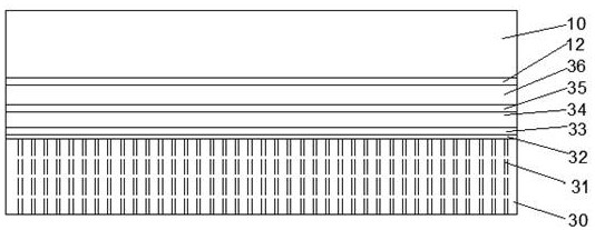
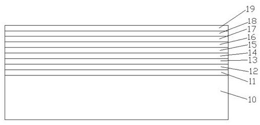
[0050] Such as Figure 1-Figure 3As shown, the present invention provides a method for transferring a solar cell substrate, comprising the following steps

[0051] S1: Growth of battery structure, using MOCVD equipment to grow battery epitaxial layer 36 on GaAs substrate 10, said battery epitaxial layer 36 includes N-GaAs buffer layer, GaInP etch stop layer 12, N-GaAs contact Layer 13 , GaInP top cell 14 , first tunnel junction 15 , GaAs middle cell 16 , second tunnel junction 17 , InGaAs bottom cell 18 and P-InGaAs contact layer 19 .

[0052] S2: Evaporate the metal bonding layer on the surface of the battery epitaxial layer 36 and the flexible substrate 34, and the grown battery epitaxial layer 36 and the flexible substrate 34 are cleaned with organic ultrasonic waves, and the battery epitaxial layer is sequentially evaporated by electron beams respectively metal bond layer 35, flexible substrate metal bond and layer 33,

[0053] Evaporation of the bonding layer of the bat...


PUM

PropertyMeasurementUnit
thicknessaaaaaaaaaa

Abstract

The invention discloses a transfer method of a solar cell substrate. The method comprises the following steps of S1, battery structure growth; S2, metal bonding layer evaporation on the surfaces of abattery epitaxial layer and a flexible substrate; S3, temporary substrate manufacturing; S4, temporary substrate bonding layer evaporation; S5, substrate transfer; S6, substrate removal; S7, device manufacturing; S8, annealing; S9, temporary substrate transfer; and S10, scribing and testing. According to the invention, the method is simple in process and convenient to operate, can effectively solve the problems of infirm bonding of temporary bonding glue, difficulty in cleaning with glue, difficulty in alloy annealing with glue and bubbling and failure of the surface of the battery caused by mismatching of expansion coefficients of the flexible substrate and the epitaxial layer after the thin-film battery is stripped, can reduce the cost of the battery, and improves the yield of the battery.

Description

technical field [0001] The invention relates to the technical field of solar cells, in particular to a method for transferring a solar cell substrate. Background technique [0002] Gallium arsenide thin-film solar cells have a better band gap matching with the full spectrum of each junction cell, which helps to fully absorb sunlight, making its photoelectric conversion efficiency far ahead of other solar cells, and its light weight, easy to bend characteristics, It is highly dependent on space power systems such as aerospace and aviation. Stratospheric airships and solar-powered unmanned aerial vehicles are mainly used in the fields of communication, resource exploration and military reconnaissance. Due to their long time in the air during the day, strong flexibility and large coverage areas, gallium arsenide thin-film batteries are an irreplaceable choice. . Improving the conversion efficiency of gallium arsenide solar cells, reducing the surface density of cells, and the...

Claims


Application Information

Patent Timeline
Patent Type & Authority Applications(China)
IPC IPC(8): H01L31/18
CPCH01L31/1844H01L31/1892H01L31/1896Y02E10/544Y02P70/50
Inventor 吴洪清米万里李俊承杨文斐孙志泉
Owner NANCHANG KAIXUN PHOTOELECTRIC CO LTD
Why Eureka
Try Eureka