

A transition layer for cigs-based thin film photovoltaic cells and preparation method thereof
A thin-film photovoltaic cell and transition layer technology, which is applied in the manufacture of circuits, electrical components, and final products, can solve the problems of insufficient bonding between the metal molybdenum electrode layer and the glass substrate, and achieve the solution of weak bonding, firm bonding, and good The effect of the transition connection
- Summary
- Abstract
- Description
- Claims
- Application Information
AI Technical Summary
Problems solved by technology
Method used
Image

Examples
Embodiment 1
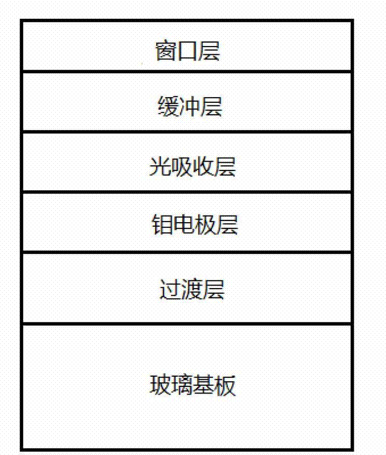
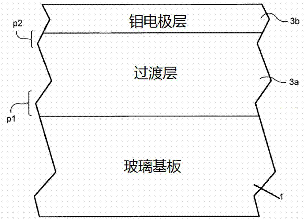
[0037] A transition layer 3 a with a thickness of 15 nm and a molybdenum electrode layer with a thickness of 400 nm are sequentially deposited on a soda lime glass substrate with a thickness of 3.0 mm. Both the transition layer 3a and the molybdenum electrode layer are deposited by magnetron sputtering, and the deposition of the transition layer 3a uses three kinds of targets: an alloy target containing 25% silicon, 70% zirconium, and 5% molybdenum is the first sputtering target. The target, the alloy target containing 35% silicon, 30% zirconium, and 35% molybdenum is the second sputtering target, and the alloy target containing 10% silicon, 5% zirconium, and 85% molybdenum is the third sputtering target. The soda-lime glass substrate is sequentially passed under the first sputtering target, the second sputtering target and the third sputtering target, and argon and oxygen are introduced during the sputtering deposition process to form each layer with a thickness of about 5 nm....
Embodiment 2
[0041] A transition layer 3 a with a thickness of 15 nm and a molybdenum electrode layer with a thickness of 400 nm are sequentially deposited on a soda lime glass substrate with a thickness of 3.0 mm. Both the transition layer 3a and the molybdenum electrode layer are deposited by magnetron sputtering, and the deposition of the transition layer 3a uses three targets: an alloy target containing 20% silicon, 70% zirconium, and 10% titanium is the first sputtering The target, the alloy target containing 35% silicon, 30% zirconium and 35% molybdenum is the second sputtering target, and the target containing 100% molybdenum is the third sputtering target. The soda-lime glass substrate is sequentially passed under the first sputtering target, the second sputtering target and the third sputtering target, and argon and nitrogen are introduced during the sputtering deposition process to form each layer with a thickness of about 5 nm. Transition layer 3a with a thickness of 15 nm. T...
Embodiment 3
[0045] A transition layer 3 a with a thickness of 15 nm and a molybdenum electrode layer with a thickness of 400 nm are sequentially deposited on a soda lime glass substrate with a thickness of 3.0 mm. Both the transition layer 3a and the molybdenum electrode layer were deposited by magnetron sputtering, and the transition layer 3a was deposited using an alloy target containing 15% silicon, 60% zirconium, and 25% molybdenum. The soda-lime glass substrate is passed under the sputtering target, and argon, oxygen and nitrogen are introduced during the sputtering deposition process to form a transition layer 3 a with a thickness of 15 nm. Thus obtained with figure 2 The transition layer of the structure shown.
[0046] Laminate coated glass, 0.76mm PVB and another 3.0mm original glass sheet to make laminated glass. Do a knock test on the laminated glass, and the level of the knock test is 3, which shows that the adhesion of the film layer to the glass substrate and PVB is very ...
PUM
| Property | Measurement | Unit |
|---|---|---|
| thickness | aaaaa | aaaaa |
| thickness | aaaaa | aaaaa |
| thickness | aaaaa | aaaaa |
Abstract
Description
Claims
Application Information