
Light-operated terahertz wave modulation device and preparation method thereof

A terahertz wave and electrode technology, applied in the field of communication, can solve the problems of inability to take advantage of the high carrier frequency and large transmission bandwidth of terahertz wave, low modulation rate, small modulation depth, etc., and achieve large carrier mobility and current carrying capacity. Effects of sub-diffusion length, sensitivity improvement, and high modulation rate

Inactive Publication Date: 2020-12-04
苏州睿翔智臻光电科技有限公司
View PDF0 Cites 2 Cited by
  • Summary
  • Abstract
  • Description
  • Claims
  • Application Information

AI Technical Summary

Problems solved by technology

[0004] The current terahertz modulation devices have the following problems: the working frequency is mainly in the low frequency and millimeter wave band; the modulation bandwidth is narrow, generally only a few GHz, and the modulation rate is low, the highest modulation rate is generally in the order of MHz, which cannot make full use of the high carrier frequency of terahertz waves. The advantage of transmission bandwidth; the modulation depth is small, generally within 50%, and this index decreases rapidly with the increase of modulation rate and operating frequency

Method used


Image

  • Light-operated terahertz wave modulation device and preparation method thereof

Examples


Embodiment Construction

[0026] In order to understand the above-mentioned purpose, features and advantages of the present invention more clearly, the present invention will be further described in detail below in conjunction with the accompanying drawings and specific embodiments. It should be noted that, in the case of no conflict, the embodiments of the present application and the features in the embodiments can be combined with each other.

[0027] In the following description, many specific details are set forth in order to fully understand the present invention. However, the present invention can also be implemented in other ways different from those described here. Therefore, the protection scope of the present invention is not limited by the specific details disclosed below. EXAMPLE LIMITATIONS.

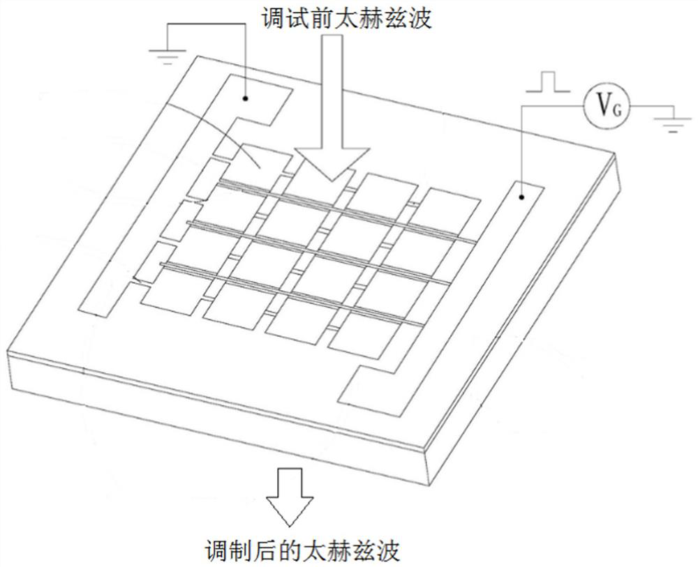
[0028] A light-controlled terahertz wave modulation device and its preparation method, comprising: a substrate, a buffer layer, a heterogeneous layer, a first electrode, a second electrode, and a vol...


PUM

PropertyMeasurementUnit
thicknessaaaaaaaaaa
thicknessaaaaaaaaaa

Abstract

The invention discloses a light-operated terahertz wave modulation device and a preparation method thereof. The light-operated terahertz wave modulation device comprises a substrate, a buffer layer, aheterogeneous layer, a first electrode, a second electrode and a voltage and current source which are arranged in sequence, wherein the voltage and current source comprises a positive electrode output end and a negative electrode output end, the substrate comprises a first surface and a second surface which are opposite to each other, the first electrode is arranged on the first surface, the second electrode is arranged on the second surface, a plurality of columns of transistors are formed on the heterogeneous layer, the plurality of columns of transistors are connected in series, ohmic electrodes of the plurality of columns of transistors are connected with the first electrode, gates of two adjacent columns of transistors are connected, the gates are connected with the second electrode,the ohmic electrodes, the gates, the first electrode and the second electrode form a composite metasurface structure, the gates regulate and control channel conductance between every two adjacent ohmic electrodes in each column, the composite metasurface structure is converted between the resonance metasurface and a wire grid, and the sensitivity of the light-operated terahertz modulation deviceis greatly improved.

Description

technical field [0001] The invention relates to the field of communication technology, in particular to an optically controlled terahertz wave modulation device and a preparation method thereof. Background technique [0002] Terahertz waves, also known as far-infrared waves, refer to electromagnetic waves with frequencies in the 0.1-10 terahertz band. Recognize and apply bands. Compared with X-rays, terahertz imaging technology and spectrum technology have more advantages due to high frequency, short pulse, strong penetrability, and low energy, and less damage to matter and human body. , security checks, broadband communications and other aspects have broad prospects. In recent years, many terahertz modulation devices have been proposed, including terahertz modulation devices based on quantum wells, photonic crystals, semiconductor silicon, and metamaterials. According to the modulation method, they can be divided into amplitude modulation, phase modulation, and frequency ...

Claims


Application Information

Patent Timeline
Patent Type & Authority Applications(China)
IPC IPC(8): G02F1/00G02F1/03
CPCG02F1/0018G02F1/0305G02F1/0316
Inventor 王冬
Owner 苏州睿翔智臻光电科技有限公司
Learn More