NAND memory and manufacturing method thereof

A manufacturing method and memory technology, applied in semiconductor/solid-state device manufacturing, electric solid-state devices, semiconductor devices, etc., can solve problems affecting the normal use of devices, affecting the connection of metal contact holes, etc.

Pending Publication Date: 2020-12-04
SHANGHAI HUALI MICROELECTRONICS CORP
View PDF0 Cites 0 Cited by
  • Summary
  • Abstract
  • Description
  • Claims
  • Application Information

AI Technical Summary

Problems solved by technology

[0003] However, in the manufacturing process of commonly used NAND memory, while air gaps are formed between word lines, voids will appear in the interlayer dielectric layer (ILD). Affect the connection of the metal contact hole, thus affecting the normal use of the device

Method used


Image

  • NAND memory and manufacturing method thereof
  • NAND memory and manufacturing method thereof
  • NAND memory and manufacturing method thereof

Examples


preparation example Construction

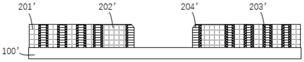
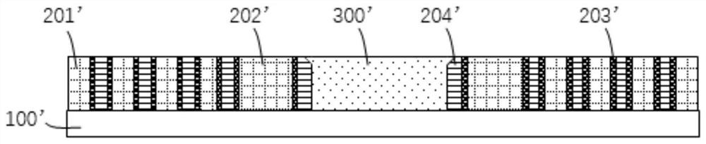
[0051] In the manufacturing method of the above-mentioned NAND memory, when the first sidewall 204' is etched, the first sidewall 204' between the selection tube 202' and the interlayer dielectric layer 300' is removed, resulting in subsequent When the air gap between the word lines 201' is formed, a void A appears in the interlayer dielectric layer 300' (ie Figure 1EIn the area indicated by A). Since the contact hole made in the subsequent manufacturing process of the NAND memory needs to pass through the interlayer dielectric layer 300' and be filled with metal, the existence of the void A will cause the connection between the contact hole and the contact hole, thereby affecting the normal use of the device.

[0052] In order to avoid the above situation, this embodiment provides a method for manufacturing a NAND memory, figure 2 It is a flow chart of the manufacturing method of the NAND memory provided by this embodiment. refer to figure 2 It can be seen that the manu...


PUM


Abstract

The invention provides an NAND memory and a manufacturing method thereof. The manufacturing method of the NAND memory comprises the steps that a substrate is provided, word lines and selection tubes which are arranged repeatedly are formed on the substrate, and first side walls are formed on the side walls of the word lines and the selection tubes; the first side walls between the adjacent selection tubes are etched to enable the upper surfaces of the first side walls between the adjacent selection tubes to be lower than the upper surfaces of the selection tubes; an interlayer dielectric layeris formed, wherein the interlayer dielectric layer covers the first side wall and the substrate between the adjacent selection tubes; the first side walls between the word lines and between the wordlines and the selection tubes are removed; and oxide layers are formed on the word lines, the selection tube and the interlayer dielectric layer so as to form air gaps among the word lines. The firstside walls between the adjacent selection tubes are partially etched before the interlayer dielectric layer is formed, so that the first side walls between the selection tubes are buried under the subsequently formed interlayer dielectric layer, the selection tubes are prevented from being removed in the process of forming the air gap, and holes are prevented from appearing in the interlayer dielectric layer.

Description

technical field [0001] The invention relates to the technical field of semiconductors, in particular to a NAND memory and a manufacturing method thereof. Background technique [0002] As a non-volatile memory, NAND memory has the advantages of large capacity, fast erasing and writing speed, and low cost. It is widely used in consumer, automobile, industrial electronics and other fields. With the development of semiconductor technology, the word line size of NAND memory is continuously shrinking to increase the data storage capacity and meet the actual use requirements. In the prior art, a NAND memory array is usually composed of multiple blocks, and each block includes several word lines and selection transistors. The select transistors are located at both ends of each block and adjacent to the word lines. NAND memory with a word line size below 30nm usually adopts an air gap technology (Air gap) between word lines to reduce the coupling effect between word lines. [0003...

Claims


Application Information

Patent Timeline
Patent Type & Authority Applications(China)
IPC IPC(8): H01L27/11524H01L27/1157H01L21/768H01L23/528
CPCH01L21/7682H01L23/5283H10B41/35H10B43/35
Inventor 姚邵康巨晓华王奇伟
Owner SHANGHAI HUALI MICROELECTRONICS CORP
Why Eureka
Try Eureka