Supercharge Your Innovation With Domain-Expert AI Agents!

Manufacturing method of self-aligned double-groove gallium arsenide field effect transistor

A technology of gallium arsenide field and fabrication method, applied in semiconductor/solid-state device manufacturing, semiconductor devices, electrical components, etc., can solve problems such as overlay offset, affecting device performance, etc., to ensure alignment, reduce process, The effect of stable device performance

Active Publication Date: 2020-12-04
XIAMEN SANAN INTEGRATED CIRCUIT
View PDF5 Cites 1 Cited by
  • Summary
  • Abstract
  • Description
  • Claims
  • Application Information

AI Technical Summary

Problems solved by technology

[0004] In the manufacturing process of T-shaped gates, it is often necessary to use overlay technology to groove the epitaxial layer and deposit gate metal. At the micro-nano line width scale, it is easy to overlay offset and affect the performance of the device.

Method used


Image

  • Manufacturing method of self-aligned double-groove gallium arsenide field effect transistor
  • Manufacturing method of self-aligned double-groove gallium arsenide field effect transistor
  • Manufacturing method of self-aligned double-groove gallium arsenide field effect transistor

Examples


Embodiment 1

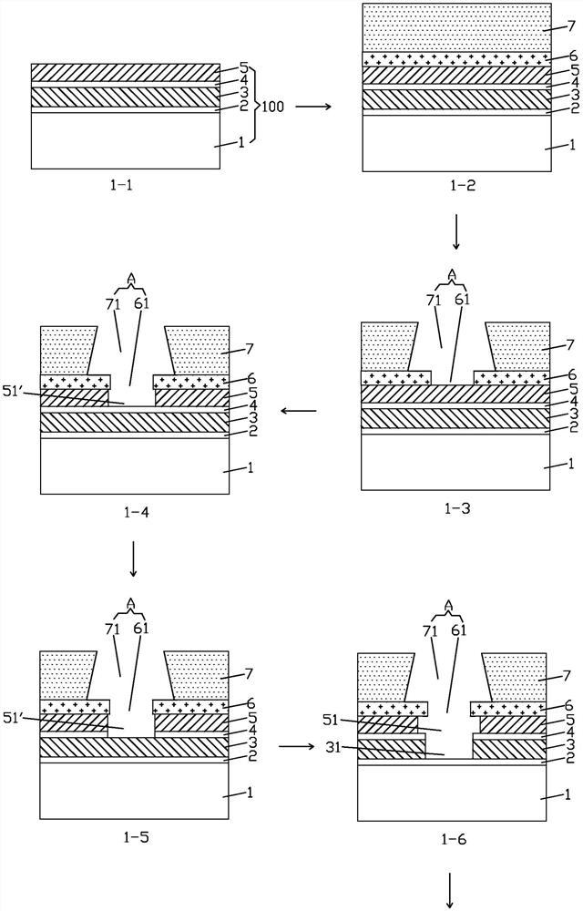
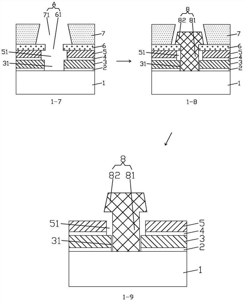
[0034] by figure 1 As an example, a method for fabricating a self-aligned double-groove GaAs field effect transistor of the present invention will be described in detail.

[0035] refer to Picture 1-1 , providing an epitaxial substrate 100 for a field effect transistor, the epitaxial substrate 100 includes an underlying structure 1, a first termination layer 2, an N-type doped GaAs layer 3, a second termination layer 4, and an N-type heavily doped GaAs layer from bottom to top 5. The underlying structure 1 includes known structures such as a substrate, a buffer layer, a channel layer, and a barrier layer, and is formed by using epitaxial materials of conventional GaAs-based field effect transistors. The N-type doped GaAs layer 3 is to increase the device breakdown voltage, and the doping concentration of the N-type doped GaAs layer 3 is 2×10 12 ~5×10 12 cm -3 , the thickness range is less than 15nm. N-type heavily doped GaAs layer 5 is used to make source and drain elec...


PUM

PropertyMeasurementUnit
Doping concentrationaaaaaaaaaa
Thicknessaaaaaaaaaa

Abstract

The invention discloses a manufacturing method of a self-aligned double-groove gallium arsenide field effect transistor. The method comprises the following steps of: forming a T-shaped window on an epitaxial substrate by adopting two different photoresists, and etching an N type heavily doped GaAs layer to form a first prefabricated groove; and then etching an N type doped GaAs layer at the bottomof the first prefabricated groove by adopting a wet etching process and simultaneously transversely etching an N type heavily doped GaAs layer on the side wall of the first prefabricated groove to enable the N type doped GaAs layer to form a second groove and enable the first prefabricated groove to be expanded to form a first groove, then depositing metal in the T-shaped window, the first grooveand the second groove to form T-shaped gates. According to the invention, the double grooves obtained by etching different termination layers twice by using the same mask morphology have extremely high alignment performance, so that the influence of an offset problem caused by an overlay technology on the performance of the device is avoided.

Description

technical field [0001] The invention relates to the technical field of semiconductor manufacturing technology, in particular to a method for manufacturing a self-aligned double-groove gallium arsenide field effect transistor. Background technique [0002] Gallium arsenide (GaAs) is a second-generation semiconductor with excellent electrical properties such as high saturation electron velocity, high electron mobility, and high breakdown voltage. With strong radiation ability, it is widely used in the fields of integrated circuits, infrared light-emitting diodes, semiconductor lasers and solar cells. Among them, gallium arsenide-based field-effect transistor (GaAs FET) has a unique structure, has the characteristics of high power gain, high efficiency, and low power, and is becoming more and more attractive in the application of transistors. [0003] The fabrication of the gate of GaAs FET has a crucial influence on the cut-off frequency of the device. Generally speaking, th...

Claims


Application Information

Patent Timeline
IPC IPC(8): H01L29/423H01L29/20H01L29/772H01L21/335
CPCH01L29/42316H01L29/772H01L29/66446H01L29/20
Inventor 何先良林志东孙希国杨宇李云燕魏明强
Owner XIAMEN SANAN INTEGRATED CIRCUIT
Features
  • R&D
  • Intellectual Property
  • Life Sciences
  • Materials
  • Tech Scout
  • Unparalleled Data Quality
  • Higher Quality Content
  • 60% Fewer Hallucinations
Learn More