Terahertz fano resonance super-structure device capable of realizing efficient light control
A terahertz fano and resonance technology, which is used in semiconductor devices, semiconductor/solid-state device manufacturing, electrical components, etc., can solve the problems of initial Fano resonance weakening, loss of Fano resonance modulation amplitude range, etc., so that the preparation process can be streamlined , The effect of large batch processing difficulty and high resonance intensity
- Summary
- Abstract
- Description
- Claims
- Application Information
AI Technical Summary
Problems solved by technology
Method used
Image
Examples
Embodiment 1
[0050] A terahertz fano resonant meta-device capable of high-efficiency light control, comprising the following steps:
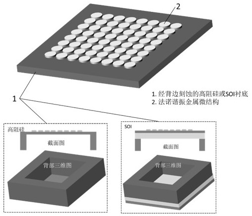
[0051] (1) Spin-coat positive photoresist on high-resistance silicon with a resistivity of 0.03 S / m, and develop a square split double split ring shape through a conventional photolithography process. The dielectric constant of high-resistance silicon is 11.9, and the shape is square with side length 14 mm and a thickness of 500 mm.
[0052] (2) Evaporate aluminum with a thickness of 200 nm by thermal evaporation. The current used in the thermal evaporation process is 40A, and the evaporation time is 30 minutes.
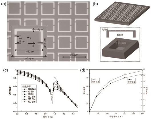
[0053] (3) Wash off the residual photoresist, and finally leave a metal microstructure with a specific shape on the high-resistance silicon or SOI substrate. The physical and structural parameters are as follows: image 3 (a).
[0054] (4) Etch the back of the high-resistance silicon by ion etching process to reduce its thickness to 3 mm, and lea...
Embodiment 2
[0057] A terahertz fano resonant meta-device capable of high-efficiency light control, comprising the following steps:
[0058] (1) Spin-coat positive photoresist on SOI to develop a square split double split ring shape. The resistivity of the top silicon of SOI is 0.03S / m, the dielectric constant is 11.9, the shape is square, the side length is 14 mm, the thickness of the top silicon is 0.5 mm, the thickness of the middle silicon dioxide insulating layer is 2-4 mm, and the thickness of the bottom silicon is is 500mm.
[0059] (2) Aluminum with a thickness of 100 nm was evaporated by thermal evaporation. The current used in the thermal evaporation process was 40A, and the evaporation time was 30 minutes.
[0060] (3) Wash off the residual photoresist, and finally leave a metal microstructure with a specific shape on the SOI substrate, which is the same as that in Example 1 image 3 (a) Same.
[0061] (4) Etch the silicon at the bottom of the SOI by an ion etching process, e...
Embodiment 3
[0064] A terahertz fano resonant meta-device capable of high-efficiency light control, comprising the following steps:
[0065] (1) Spin-coat positive photoresist on SOI to develop an asymmetric nested circular shape in the ring. The resistivity of the top silicon of SOI is 0.03 S / m, the dielectric constant is 11.9, the shape is square, the side length is 14 mm, the thickness of the top silicon is 0.5 mm, the thickness of the middle silicon dioxide insulating layer is 2-4 mm, and the thickness of the bottom silicon is is 500 mm.
[0066] (2) Plating gold with a thickness of 300 nm by magnetron sputtering, the sputtering current is 15A, and the evaporation time is 8 minutes.
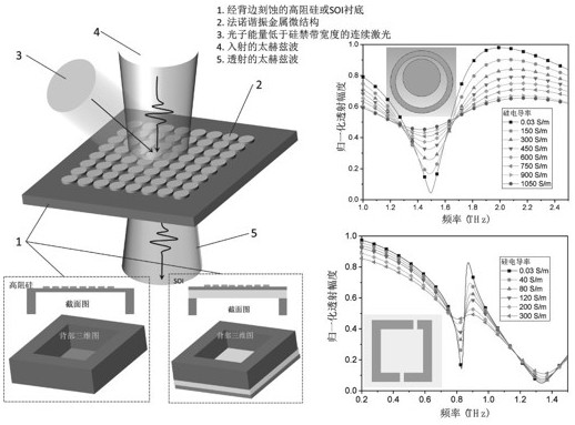
[0067] (3) Wash off the residual photoresist, and finally leave a metal microstructure with a specific shape on the SOI substrate. This structure is shown as Figure 5 (a).
[0068] (4) Etch the silicon at the bottom of the SOI by an ion etching process, etch all of it, leaving only the top silicon and...
PUM
| Property | Measurement | Unit |
|---|---|---|
| Thickness | aaaaa | aaaaa |
| Thickness | aaaaa | aaaaa |
| Thickness | aaaaa | aaaaa |
Abstract
Description
Claims
Application Information


