Light-emitting diode and manufacturing method thereof

A technology of light-emitting diodes and manufacturing methods, which is applied in the direction of electrical components, circuits, semiconductor devices, etc., can solve the problems of poor current spreading effect and large internal resistance of light-emitting diodes, and achieve fewer failed particles, reduce square resistance, and facilitate production Effect

Inactive Publication Date: 2020-12-25
XIAMEN CHANGELIGHT CO LTD
View PDF13 Cites 0 Cited by
  • Summary
  • Abstract
  • Description
  • Claims
  • Application Information

AI Technical Summary

Problems solved by technology

[0005] The purpose of the present invention is to provide a light-emitting diode and its manufacturing method to solve the problems of poor internal current expansion effect and large internal resistance of light-emitting diodes

Method used


Image

  • Light-emitting diode and manufacturing method thereof
  • Light-emitting diode and manufacturing method thereof
  • Light-emitting diode and manufacturing method thereof

Examples


Embodiment 1

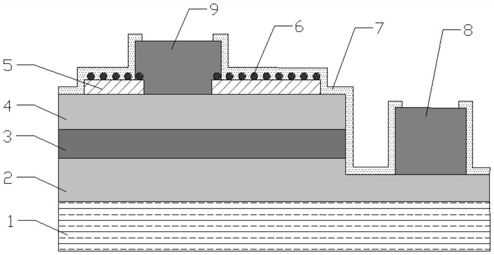
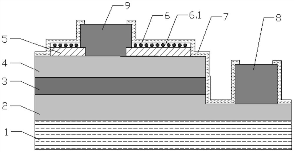
[0058] like figure 1 As shown, a light-emitting diode, the light-emitting diode is a horizontal structure, which includes:

[0059] substrate1;

[0060] A light-emitting structure A disposed on the surface of a substrate 1; the light-emitting structure A at least includes a first-type semiconductor layer 2, an active region 3, and a second-type semiconductor layer 4 stacked in sequence along a first direction; the first direction is perpendicular to the substrate 1 , and point to the light-emitting structure A from the substrate 1;

[0061] The nanosystem, the nanosystem is laminated on at least one surface of the light-emitting structure A, and the free vibration frequency of the nanosystem matches the photon frequency of the incident light of the light-emitting structure A; optionally, the free vibration frequency of the nanosystem is greater than or equal to the specified The incident light photon frequency of the light-emitting structure induces the electrons of the nano...

Embodiment 2

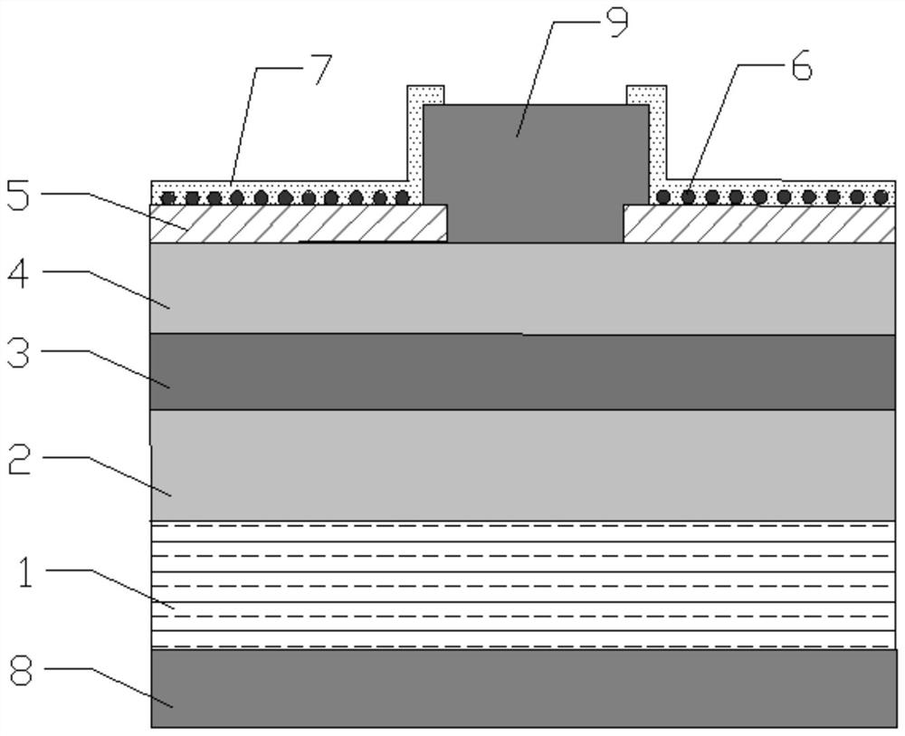
[0096] like image 3 As shown, a light-emitting diode, the light-emitting diode is a vertical structure, which includes:

[0097] substrate1;

[0098]A light-emitting structure A disposed on the surface of a substrate 1; the light-emitting structure A at least includes a first-type semiconductor layer 2, an active region 3, and a second-type semiconductor layer 4 stacked in sequence along a first direction; the first direction is perpendicular to the substrate 1 , and point to the light-emitting structure A from the substrate 1;

[0099] A nanosystem, where the nanosystem is stacked on at least one surface of the light-emitting structure A, and the free vibration frequency of the nanosystem matches the photon frequency of the incident light of the light-emitting structure A;

[0100] The first electrode 8, the first electrode 8 is stacked on the surface of the light emitting structure A, and forms an ohmic contact with the second type semiconductor layer 4;

[0101] The sec...


PUM

PropertyMeasurementUnit
refractive indexaaaaaaaaaa

Abstract

The invention provides a light-emitting diode and a manufacturing method thereof. A nano system is constructed on the surface of a light-emitting structure, and the free vibration frequency of the nano system is matched with the incident light photon frequency of the light-emitting structure, so that a localized surface plasmon resonance (LSPR) effect is formed on the local surface of the light-emitting structure, and the brightness of the light-emitting diode is improved. Through the application of a nanoimprint lithography process, the formation of equidistant and uniform nano-particles canbe accurately controlled, and the number of invalid particles is small, so that an optimal nano-system is obtained; and meanwhile, the process is simple and convenient, and production is facilitated.

Description

technical field [0001] The invention relates to the field of light emitting diodes, in particular to a light emitting diode and a manufacturing method thereof. Background technique [0002] With the rapid development of LED technology and the gradual improvement of LED light efficiency, the application of LED is becoming more and more extensive, and people are paying more and more attention to the development prospect of LED in display screens. LED chip, as the core component of LED lamp, its function is to convert electrical energy into light energy, specifically, it includes epitaxial wafers and N-type electrodes and P-type electrodes respectively arranged on the epitaxial wafers. The epitaxial wafer includes a P-type semiconductor layer, an N-type semiconductor layer, and an active layer between the N-type semiconductor layer and the P-type semiconductor layer. When a current passes through the LED chip, the holes in the P-type semiconductor and The electrons in the N-ty...

Claims


Application Information

Patent Timeline
Patent Type & Authority Applications(China)
IPC IPC(8): H01L33/14H01L33/36H01L33/00
CPCH01L33/24H01L33/14H01L33/36H01L33/005
Inventor 张书山邬新根周弘毅刘英策王锐
Owner XIAMEN CHANGELIGHT CO LTD
Why Eureka
Try Eureka