Semiconductor laser chip capable of resisting electrostatic shock and process
An electrostatic shock and semiconductor technology, applied in the field of semiconductor laser chips and processes, can solve the threat of electrostatic shock to optical chips, weak and unavoidable anti-static shock capabilities, and improve the ability to resist ESD. The chip process is simple and improved. Effect of high temperature characteristics
- Summary
- Abstract
- Description
- Claims
- Application Information
AI Technical Summary
Problems solved by technology
Method used
Image

Examples
Embodiment Construction
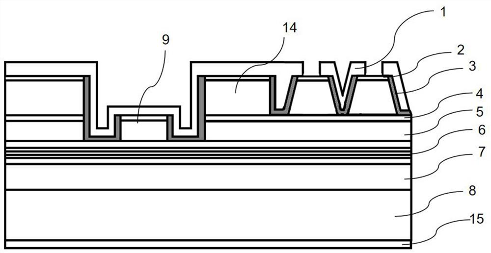
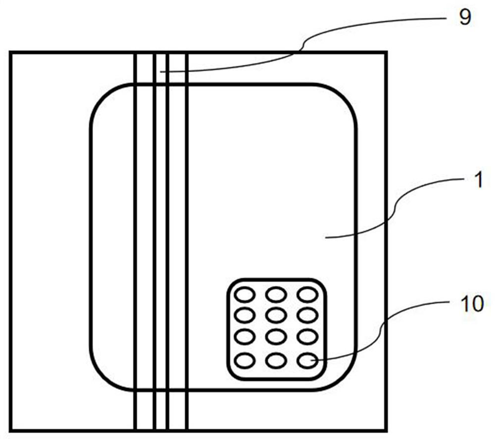
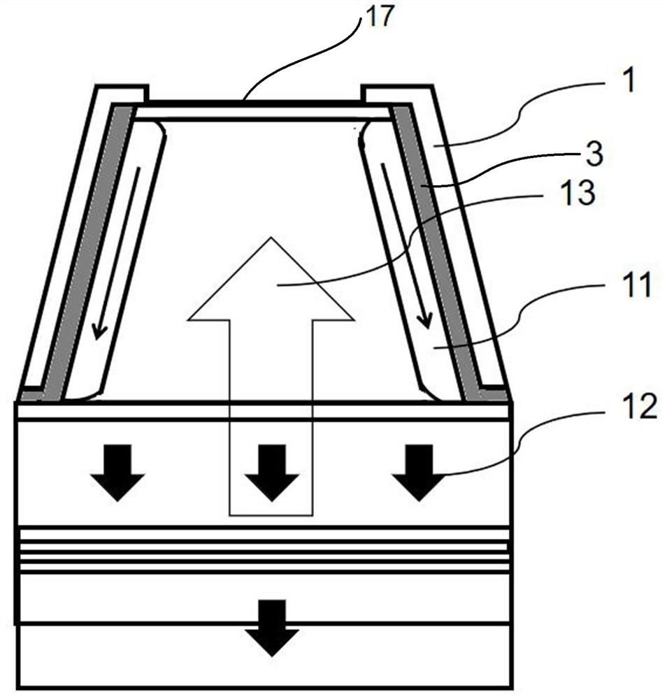
[0054] In order to make the object, technical solution and advantages of the present invention clearer, the present invention will be further described in detail below in conjunction with the accompanying drawings and embodiments. It should be understood that the specific embodiments described here are only used to explain the present invention, not to limit the present invention.
[0055] It should be noted that the implementation manners not shown or described in the accompanying drawings are forms known to those skilled in the art. Additionally, while illustrations of parameters containing particular values are provided herein, it should be understood that the parameters need not be exactly equal to the corresponding values, but rather may approximate the corresponding values within acceptable error margins or design constraints. In addition, parameters such as specific materials and thicknesses mentioned in the following embodiments are only for illustration and not fo...
PUM
| Property | Measurement | Unit |
|---|---|---|
| Thickness | aaaaa | aaaaa |
| Doping concentration | aaaaa | aaaaa |
| Doping concentration | aaaaa | aaaaa |
Abstract
Description
Claims
Application Information
 - Generate Ideas
- Intellectual Property
- Life Sciences
- Materials
- Tech Scout
- Unparalleled Data Quality
- Higher Quality Content
- 60% Fewer Hallucinations
Browse by: Latest US Patents, China's latest patents, Technical Efficacy Thesaurus, Application Domain, Technology Topic, Popular Technical Reports.
© 2025 PatSnap. All rights reserved.Legal|Privacy policy|Modern Slavery Act Transparency Statement|Sitemap|About US| Contact US: help@patsnap.com