Method and system for machining micro-nano structure with array anti-reflection function

A technology of micro-nano structure and processing method, which is applied in the direction of metal processing equipment, manufacturing tools, welding equipment, etc., can solve the problems of low efficiency, poor precision and consistency, and achieve the goal of improving preparation efficiency, improving manufacturing efficiency, and flexible manufacturing means Effect

Active Publication Date: 2021-01-08
XI'AN INST OF OPTICS & FINE MECHANICS - CHINESE ACAD OF SCI
View PDF6 Cites 1 Cited by
  • Summary
  • Abstract
  • Description
  • Claims
  • Application Information

AI Technical Summary

Problems solved by technology

[0006] In order to solve the problems of low efficiency, poor precision and poor consistency in the anti-reflection and anti-reflection micro-nano structure processing method of large-format transparent curved surface components by laser single-point processing, the present invention provides a micro-nano structure processing method for array anti-reflection and anti-reflection functions

Method used


Image

  • Method and system for machining micro-nano structure with array anti-reflection function
  • Method and system for machining micro-nano structure with array anti-reflection function
  • Method and system for machining micro-nano structure with array anti-reflection function

Examples


Embodiment 1

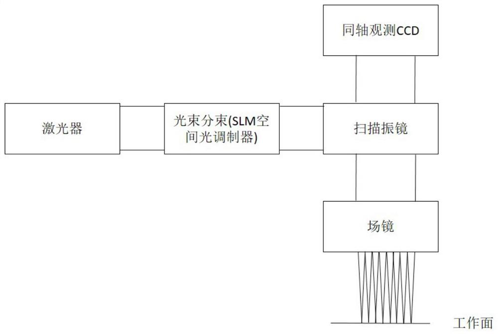
[0081] The system composition used in this embodiment is as follows: figure 1 As shown, it is composed of laser, SLM spatial light modulator, scanning galvanometer, field mirror and coaxial observation CCD and other components. In other embodiments, the field lens can also be replaced by a microscope objective lens.

[0082] The output laser light of the laser enters the SLM spatial light modulator, and the SLM spatial light modulator divides the laser beam into array processing beams, which are reflected to the field mirror by the scanning galvanometer, and the array processing beams are focused to the working surface by the field mirror, realizing the array micro nanostructure processing.

[0083] The specific method is realized through the following steps:

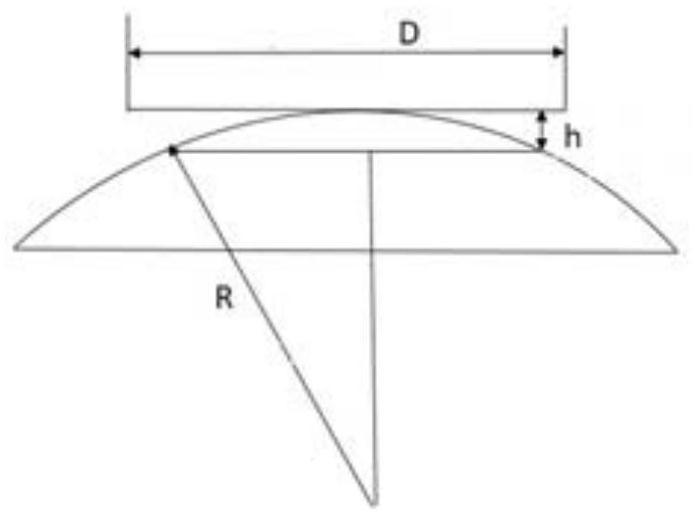
[0084] (1) Carry out process tests to determine the adjustable range h of each micro-nano structure. The micro-nano structure can be a blind hole on the surface of the workpiece, and the radial section of the hole ca...

Embodiment 2

[0112] The system adopted in this embodiment adds a Fesnel lens on the basis of the embodiment, and the laser is shaped into an array Bessel processing beam through the SLM spatial light modulator, and the array Bessel processing beam is realized by superimposing the Fesnel lens. Not at the same position (realize three-dimensional shaping of laser space), the working surface of the beam is directly shaped into a shape distributed along the surface shape of the component. Compared with the first embodiment, the processing process does not need to consider the manufacturing adjustable range h. like Figure 8 shown.

[0113] The specific method is realized through the following steps:

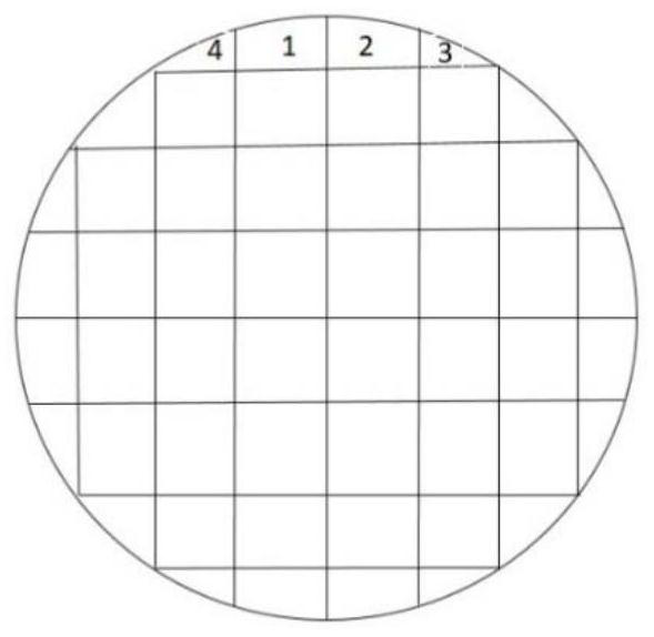
[0114] (1) Divide the surface part to be processed into several sub-regions:

[0115] like Figure 8 In b, based on the requirement that the scanning galvanometer can scan the maximum range D at one time, the curved surface part is divided into several sub-areas, and the maximum side length L o...


PUM


Abstract

The invention relates to a method and a system for machining a micro-nano structure with an array anti-reflection function. According to the method and system, the problems that the efficiency is lowand the precision and consistency are poor in the anti-reflection micro-nano structure of a large-breadth transparent curved surface component achieved through laser single-point machining are solved.The method comprises the steps of determining the manufacturing focal depth h of each micro-nano structure; segmenting the surface of a to-be-machined curved surface part into a plurality of sub-regions; determining the number of machining light beams in the array machining light beams when each sub-region is machined; laser beam splitting shaping; and machining each sub-region in sequence, and machining an edge region. The system comprises a laser, and an SLM spatial light modulator, a Fresnel lens group, a scanning galvanometer and a field lens which are sequentially arranged in an emergentlight path of the laser. By utilizing the system and the method provided by the invention, the manufacturing efficiency of the array microstructure can be greatly improved.

Description

technical field [0001] The invention relates to a micro-nano structure processing method and system for array anti-reflection and anti-reflection functions. Background technique [0002] In order to ensure the performance of high-speed aircraft fairings, various tracking and measurement photoelectric systems, and high-precision sensor optical windows, anti-reflection and anti-reflection processing must be performed on their optical windows to improve the accuracy of their working wavelengths. transmittance. The traditional coating technology has the defects of narrow transmission spectrum band and incident angle range; and due to the harsh service environment, and the interface bonding of the film layer, the difference in thermal expansion coefficient between the film layer and the substrate, the film layer and the substrate Due to the matching of the refractive index and other reasons, the film layer falls off at high and low temperature, and the service life is limited. ...

Claims


Application Information

Patent Timeline
IPC IPC(8): B23K26/362B23K26/70
CPCB23K26/362B23K26/702
Inventor 李明李珣刘红军李晨晨
Owner XI'AN INST OF OPTICS & FINE MECHANICS - CHINESE ACAD OF SCI
Why Eureka
Try Eureka