Semiconductor device, forming method thereof and image sensor
A semiconductor and device technology, applied in the field of image sensors, semiconductor devices and their formation, can solve the problem of low cost performance
- Summary
- Abstract
- Description
- Claims
- Application Information
AI Technical Summary
Problems solved by technology
Method used
Image

Examples
Embodiment Construction
[0066] Based on the above studies, embodiments of the present invention provide a semiconductor device, a method for forming the same, and an image sensor. The present invention will be described in further detail below in conjunction with the accompanying drawings and specific embodiments. The advantages and features of the present invention will become clearer from the following description. It should be noted that the drawings are all in a very simplified form and use imprecise scales, and are only used to facilitate and clearly assist the purpose of illustrating the embodiments of the present invention.
[0067] An embodiment of the present invention provides a method for forming a semiconductor device, such as figure 1 shown, including:
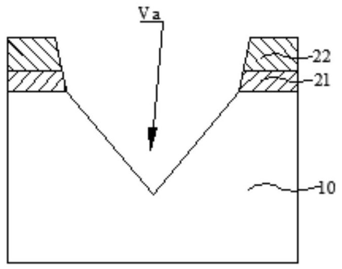
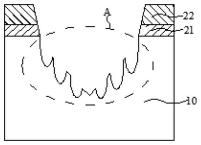
[0068] S1. Provide a substrate, and form densely distributed inverted triangular grooves on one side of the substrate; on a cross section perpendicular to the substrate, the cross-sectional shape of the inverted triangular grooves is a...
PUM
| Property | Measurement | Unit |
|---|---|---|
| reflectance | aaaaa | aaaaa |
| reflectance | aaaaa | aaaaa |
Abstract
Description
Claims
Application Information
 - R&D
- Intellectual Property
- Life Sciences
- Materials
- Tech Scout
- Unparalleled Data Quality
- Higher Quality Content
- 60% Fewer Hallucinations
Browse by: Latest US Patents, China's latest patents, Technical Efficacy Thesaurus, Application Domain, Technology Topic, Popular Technical Reports.
© 2025 PatSnap. All rights reserved.Legal|Privacy policy|Modern Slavery Act Transparency Statement|Sitemap|About US| Contact US: help@patsnap.com