
A method for detecting BGA solder balls used in integrated circuit packaging

A detection method and electronic packaging technology, applied in the direction of measuring electricity, measuring devices, measuring electrical variables, etc., can solve the problems of BGA solder joint cracking, low qualification rate, and unwelded solder joints, and reduce unwelded solder joints. , Improve the qualification rate, the effect of the detection index system

Active Publication Date: 2022-06-21
泰安晶品新材料科技有限公司
View PDF16 Cites 0 Cited by
  • Summary
  • Abstract
  • Description
  • Claims
  • Application Information

AI Technical Summary

Problems solved by technology

Due to the small size and high precision requirements of BGA packaging solder balls, solder ball preparation technology and detection technology have always been the main reasons for restricting the development of this industry.
Insufficient solder ball detection will lead to defects such as unsoldered solder joints, jumping balls, voids, and solder joint offsets during the ball planting process, causing component failures and serious accidents
For example, in 2014, the Airbus A320-216 AirAsia QZ8501 crashed in Surabaya, the second largest city in Indonesia, on its way to Singapore. On December 1, 2015, after nearly a year of investigation by the Indonesian National Transportation Safety Committee, it was found that the aircraft rudder The BGA solder joints on the A and B channel circuit boards in the control unit module (RTLU) cracked, causing the electrical connection of the instrument to be disconnected, which in turn caused the entire control unit to fail
Some domestic scientific research institutes and enterprises have made some progress in the research on BGA. In recent years, domestic BGA solder balls have gradually come out. Only applicable to low-end industries such as rework

Method used


Image

  • A method for detecting BGA solder balls used in integrated circuit packaging
  • A method for detecting BGA solder balls used in integrated circuit packaging
  • A method for detecting BGA solder balls used in integrated circuit packaging

Examples


Embodiment 1

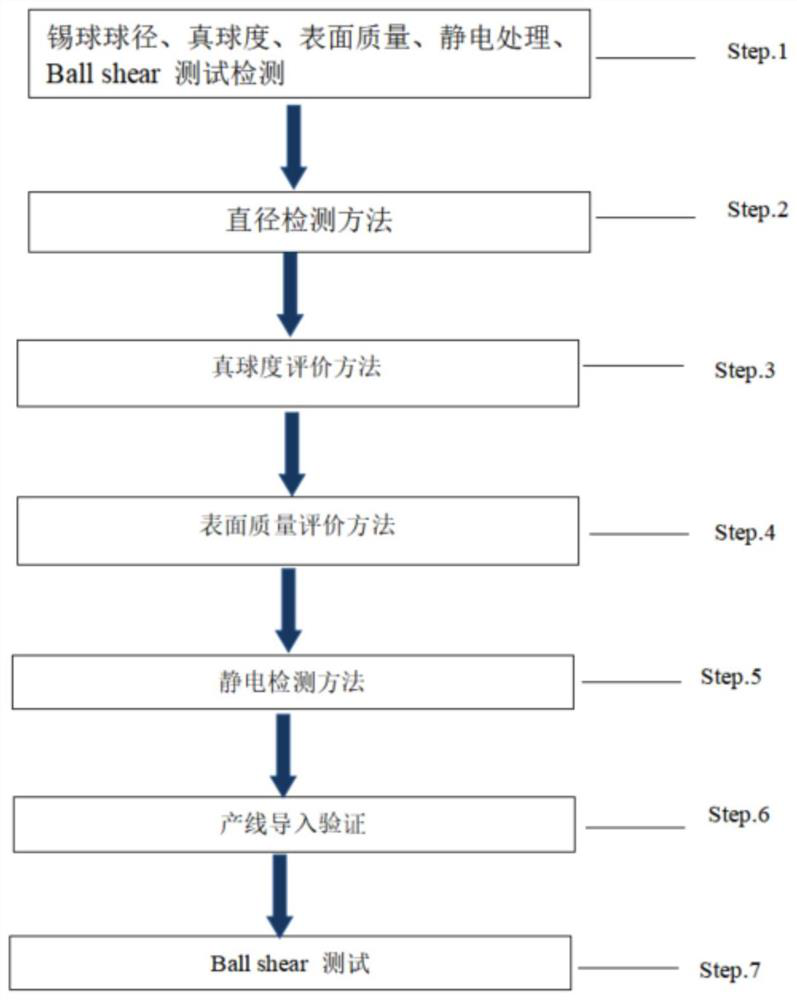
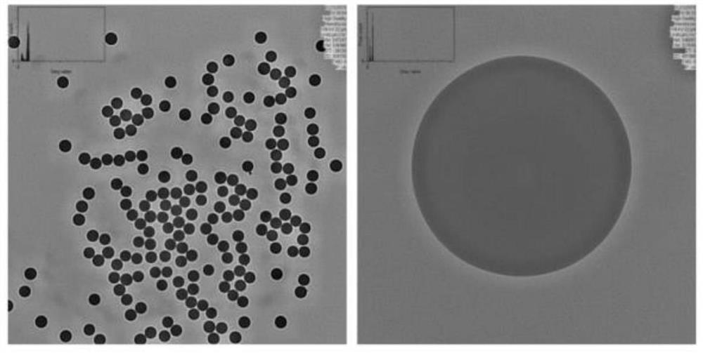
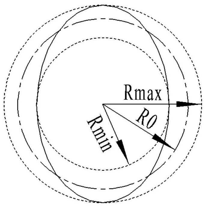
[0018] like Figure 1 to Figure 5 As shown, the present invention discloses a method for detecting BGA solder balls for integrated circuit packaging. ; The method includes Step.1, Step.2, Step.3, Step.4, Step.5, and Step.6; the Step.1 is diameter detection, specifically, the X-Ray method is used to test the diameter of the solder ball. In order to improve the detection efficiency and accuracy, the X-Ray magnification is 100-200 times. The diameter of each solder ball is tested three times and the average value is the final result. The allowable range of the diameter error of a single solder ball is ±0.02mm, and the error range of the average solder ball diameter is ±0.01mm; the Step.2 is the evaluation of sphericity, specifically, the maximum and minimum diameters of the solder ball are used for the calculation of the sphericity of the solder ball. The ratio of the difference between the diameters and the theoretical diameter is calculated, and the sphericity calculation met...

Embodiment 2

[0026] Example 2 is the same as Example 1, the difference is that the diameter of the tin ball and the parameters of the ball are different

Embodiment 3

[0028] Example 3 has the same steps as Example 1, the difference is that the diameter of the solder ball and the parameters of ball placement are different.

[0029]In order to further illustrate the present invention, the test results under three different ball-planting parameters of Example 2 and Example 3 are attached. The specific difference is that: the tin balls in the embodiment 1 are tin balls from Senju Metal Co., Ltd. of Japan, and the diameter of the tin balls is 0.25 mm. Example 2 is a self-made tin ball, the diameter of the tin ball is 0.25mm, the reflow temperature is 260 degrees, the smoothness and flatness of the tin ball are high under the magnification of 150 times, and any impurities and other contaminants, scratches, and depressions cannot be seen with the naked eye. , convex nodules, pores and slits, etc., the surface of the tin ball has no serious oxidation phenomenon, and the surface oxygen content is 7%. The ion blower blows at room temperature for 20 ...


PUM

PropertyMeasurementUnit
thicknessaaaaaaaaaa

Abstract

The invention discloses a method for detecting BGA solder balls for integrated circuit packaging, including Step.1, Step.2, Step.3, Step.4, Step.5, Step.6 and Step.7; the Step. 1 includes solder ball diameter, true sphericity, surface quality, electrostatic treatment and Ball shear test; said Step.1 includes solder ball diameter, true sphericity, surface quality, electrostatic treatment and Ball shear test; said Step.2 is the diameter detection, specifically, the X-Ray method is used to test the ball diameter. The invention detects the solder ball diameter, true sphericity, surface quality evaluation, electrostatic treatment, production line introduction verification, Ball shear, etc., and the detection indicators are more systematic and comprehensive. Reduce defects such as unwelded solder joints, jumping balls, voids, and solder joint offsets during the ball planting process, and comprehensively improve the pass rate after ball planting, so that the tested BGA solder balls can be applied to higher-end packaging fields.

Description

technical field [0001] The invention relates to the technical field of integrated circuit packaging, in particular to a method for detecting BGA solder balls for integrated circuit packaging. Background technique [0002] The full name of BGA is BallGridArray (PCB with ball grid array structure). This method has the advantages of less packaging area; increased function and increased number of pins; self-centering of PCB board during soldering, easy to tin; high reliability; good electrical performance , the overall low cost and other characteristics, the application is more and more extensive. Developed countries such as Europe, America, Japan and South Korea have carried out research on BGA solder balls earlier, including ball making equipment, ball making technology and solder ball detection methods. At present, taking advantage of technical advantages, the production and sales of large-scale electronic products such as memory, CPU, and digital signal processor, Leading t...

Claims


Application Information

Patent Timeline
Patent Type & Authority Patents(China)
IPC IPC(8): G01B21/10G01B21/20G01B15/00G01B11/24G01N23/2251G01N33/2022G01N25/00G01R31/00G01N19/00
CPCG01B21/10G01B21/20G01B15/00G01B11/24G01N23/2251G01N33/2022G01N25/00G01R31/00G01N19/00
Inventor 唐坤王广欣马庆王要利王钰森
Owner 泰安晶品新材料科技有限公司
Learn More