Method for rapidly and accurately determining crystal axis orientation of gallium oxide monocrystals

An accurate measurement and gallium oxide technology, applied in the field of gallium oxide single crystal processing, can solve the problems of inaccuracy and slow detection, and achieve the effects of low technical requirements, weakened equipment dependence, and less crystal loss.

Active Publication Date: 2021-02-23
北京铭镓半导体有限公司
View PDF7 Cites 3 Cited by
  • Summary
  • Abstract
  • Description
  • Claims
  • Application Information

AI Technical Summary

Problems solved by technology

[0009] In order to solve the technical problems of slow and inaccurate detection in related technologies, especially in the determination of crystal axis orientation of gallium oxide crystals whose crystal axis orientation is completely uncertain, This application provides a method for quickly and accurately determining the crystallographic axis orientation of a gallium oxide single crystal

Method used


Image

  • Method for rapidly and accurately determining crystal axis orientation of gallium oxide monocrystals
  • Method for rapidly and accurately determining crystal axis orientation of gallium oxide monocrystals
  • Method for rapidly and accurately determining crystal axis orientation of gallium oxide monocrystals

Examples


Embodiment 1

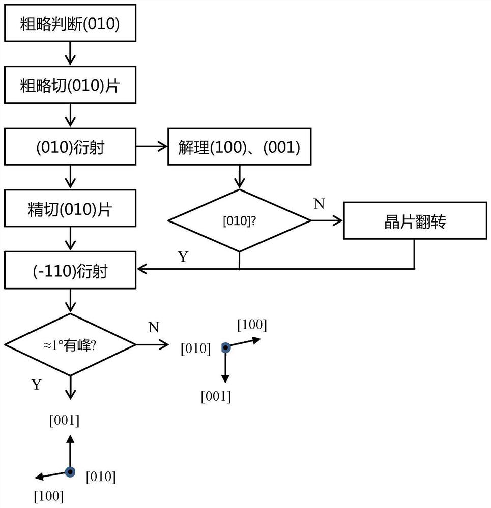
[0068] This embodiment provides an example of a method for quickly and accurately determining the crystallographic axis orientation of a gallium oxide single crystal, referring to figure 1 , the method includes the following steps:

[0069] S1. Preliminary judgment of the direction of the (010) crystal plane: take a gallium oxide crystal ingot to be tested, observe the surface of the gallium oxide crystal ingot, the plane perpendicular to the crystal fiber is the initial (010) crystal plane; among them, the gallium oxide crystal The choice of ingot is β-Ga 2 o 3 single crystal.

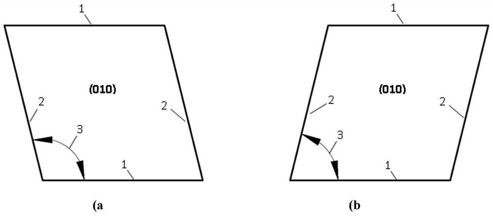
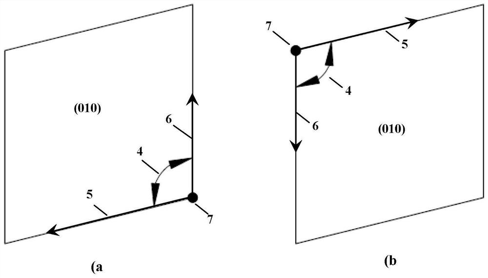
[0070] S2. Cutting the initial (010) crystal plane: fix the gallium oxide crystal ingot on the stage of the diamond wire cutting machine, and cut a small slice of crystal from the gallium oxide crystal ingot along the initial (010) crystal plane, denoted as S2 .1 Gallium oxide wafer, S2.1 The thickness of the gallium oxide wafer is 0.3 mm, and the cut gallium oxide ingot is recorded as the second g...

Embodiment 2

[0085] The difference between this embodiment and embodiment 1 is that the operating parameters and intermediate results of some steps in the detection process of the method are different, specifically including the following steps:

[0086] S1. Preliminary determination of the direction of the (010) crystal plane: the same as in Example 1;

[0087] S2. Cutting the initial (010) crystal plane: fix the gallium oxide crystal ingot on the stage of the diamond wire cutting machine, and cut a small slice of crystal from the gallium oxide crystal ingot along the initial (010) crystal plane, denoted as S2 .1 Gallium oxide wafer, S2.1 The thickness of the gallium oxide wafer is 1 mm, and the cut gallium oxide ingot is recorded as the second gallium oxide ingot;

[0088] S3. Determination of the declination angle of the initial (010) crystal plane: place the cut S2.1 gallium oxide wafer on the stage of the X-ray orientation instrument for X-ray diffraction to measure the angle between ...

Embodiment 3

[0099] The difference between this embodiment and embodiment 1 is that the operating parameters and intermediate results of some steps in the detection process of the method are different, specifically including the following steps:

[0100] S1. Preliminary determination of the direction of the (010) crystal plane: the same as in Example 1;

[0101] S2. Cutting the initial (010) crystal plane: fix the gallium oxide crystal ingot on the stage of the diamond wire cutting machine, and cut a thin slice of crystal from the gallium oxide crystal ingot along the initial (010) crystal plane, denoted as S2. 1 Gallium oxide wafer, S2.1 The thickness of the gallium oxide wafer is 0.4 mm, and the cut gallium oxide ingot is recorded as the second gallium oxide ingot;

[0102] S3. Determination of the declination angle of the initial (010) crystal plane: place the cut S2.1 gallium oxide wafer on the stage of the X-ray orientation instrument for X-ray diffraction to measure the angle between...


PUM

PropertyMeasurementUnit
thicknessaaaaaaaaaa
thicknessaaaaaaaaaa

Abstract

The invention relates to the technical field of gallium oxide monocrystal processing, and particularly discloses a method for rapidly and accurately determining a crystal axis orientation of gallium oxide monocrystals. The method comprises the following steps: S1, preliminarily judging (010) a crystal plane direction; S2, cutting the initial (010) crystal plane to obtain an S2.1 gallium oxide wafer; S3, determining an initial (010) crystal plane deflection angle by an X-ray diffractometer; S4, precisely cutting the (010) crystal plane to obtain an S4.1 gallium oxide wafer; S5, determining (100) and (001) crystal planes of the S2.1 gallium oxide wafer by a cleavage method; S6, determining the [010] crystal axis direction according to the traces of the (100) and (001) crystal planes of the S2.1 gallium oxide wafer; and S7, determining the directions of [001] and [100] crystal axes of the S2.1 gallium oxide wafer by using an X-ray orientation instrument. The method has the advantage thatthe gallium oxide crystal axis orientation in any unknown crystal direction can be rapidly and accurately determined.

Description

technical field [0001] This application relates to the technical field of gallium oxide single crystal processing, more specifically, it relates to a method for quickly and accurately measuring the crystal axis orientation of gallium oxide single crystal. Background technique [0002] A New Generation of Semiconductor Material β-Ga 2 o 3 The bandgap width is 4.9eV, and it has the advantages of high breakdown field strength, low energy consumption, and high stability, and has broad application prospects in the fields of high temperature, high frequency, and high power power electronic devices. Ga 2 o 3 Compared with other fourth-generation semiconductor materials, crystal has the advantages of larger band gap, shorter absorption cut-off edge, lower growth cost (it can be grown by melt method), and more stable physical and chemical properties. It is ideal for making ultra-high voltage power devices, The preferred material for semiconductor devices such as deep ultraviolet ...

Claims


Application Information

Patent Timeline
Patent Type & Authority Applications(China)
IPC IPC(8): G01N23/20008G01N23/20025G01N23/20016G01N1/28
CPCG01N23/20008G01N23/20025G01N23/20016G01N1/286G01N2001/2873
Inventor 陈政委吴忠亮范钦明
Owner 北京铭镓半导体有限公司
Why Eureka
Try Eureka