Millimeter-wave high-gain and high-radiation-efficiency slot antenna array based on ridge gap waveguide

A technology of gap waveguide and millimeter wave, which is applied in the direction of antenna array, antenna, radiation element structure, etc., can solve the problems of increased processing cost and high processing precision requirements, and achieve the goal of reducing processing cost, reducing weight and high radiation efficiency Effect

Active Publication Date: 2021-03-02
NANJING UNIV OF SCI & TECH
View PDF3 Cites 11 Cited by
  • Summary
  • Abstract
  • Description
  • Claims
  • Application Information

AI Technical Summary

Problems solved by technology

M.Ferrando-Rocher et al proposed an antenna array based on a ridge-gap waveguide structure ("M. Ferrando-Rocher, J.I. Herranz-Herruzo, A. Valero-Nogueira and B. Bernardo-Clemente, "Full-MetalK-Ka Dual-Band Shared-Aperture Array Antenna Fed by Combined Ridge-Groove GapWaveguide," IEEE Antennas Wireless Propag. Lett., vol. 18, no. 7, pp. 1463-1467, July 2019."), the bottom layer is based on the ridge-gap waveguide feed Although the antenna array achieves high gain and high radiation efficiency within the bandwidth, the entire antenna array is made of all metal, and because the size of the antenna array in the high frequency band is small, the processing accuracy is very high, resulting in increased processing costs. Big

Method used


Image

  • Millimeter-wave high-gain and high-radiation-efficiency slot antenna array based on ridge gap waveguide
  • Millimeter-wave high-gain and high-radiation-efficiency slot antenna array based on ridge gap waveguide
  • Millimeter-wave high-gain and high-radiation-efficiency slot antenna array based on ridge gap waveguide

Examples


Embodiment Construction

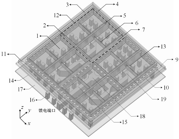
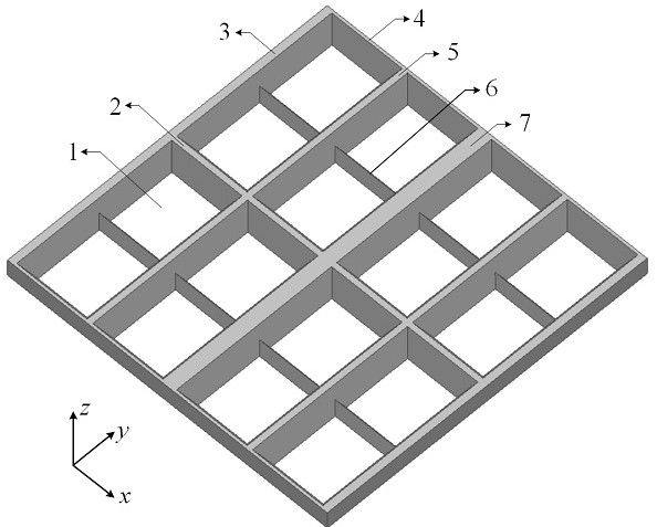
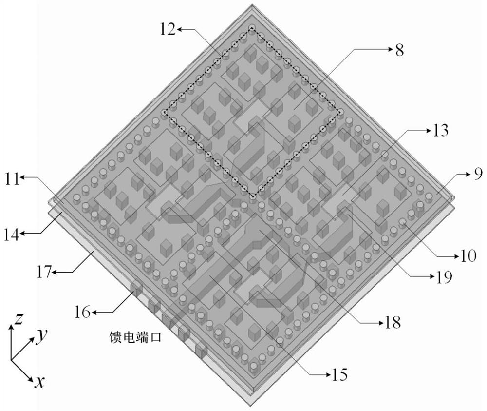
[0021] As shown in Figure 1(a), the millimeter-wave high-gain and high-radiation-efficiency slot antenna array based on the ridge-gap waveguide of the present invention includes an upper, middle and lower three-layer structure, as shown in Figure 1(b) and (c):

[0022] The uppermost layer is the radiating unit layer, which contains 16 radiating units 1 with inverted trapezoidal grooves of the same size, and metal strips 2, 3, 4, 5, 6, 7 periodically separate the 16 radiating units 1 with inverted trapezoidal grooves. The middle layer is a substrate integrated waveguide high-order mode resonant cavity feed layer processed by multi-layer printed circuit board technology. It consists of a three-layer planar structure from top to bottom, and the metal plate, dielectric substrate and metal printing surface are closely spaced. Fitting; on the top is a metal printing surface 9 with 16 rectangular slits 8, and the 16 rectangular slits 8 are aligned with the bottom surface of the bottom...


PUM


Abstract

The present invention discloses a millimeter-wave high-gain and high-radiation-efficiency slot antenna array based on a ridge gap waveguide. The millimeter-wave high-gain high-radiation-efficiency slot antenna array comprises an upper layer structure, a middle layer structure and a lower layer structure, wherein the uppermost layer is an all-metal radiation unit layer manufactured through machining and is composed of 16 inverted trapezoidal slot radiation units at equal intervals; the middle layer is a substrate integrated waveguide high-order mode resonant cavity feed layer processed by a multilayer printed circuit board technology, and the substrate integrated waveguide high-order mode resonant cavity feed layer is composed of an upper planar structure, a middle planar structure and a lower planar structure. A metal printing surface with rectangular gaps is arranged above the substrate integrated waveguide high-order mode resonant cavity feed layer. A dielectric substrate with periodically arranged metal through holes is arranged in the middle, and a metal plate with four rectangular coupling holes is arranged below the dielectric substrate; and the bottommost layer is a machinedridge gap waveguide feed network layer and comprises a metal ridge line, metal pins surrounding the metal ridge line and a metal bottom plate. The whole antenna array is small in size, light in weight and high in integration level, and high gain and high radiation efficiency are realized in a working bandwidth.

Description

technical field [0001] The invention belongs to millimeter-wave integrated antenna arrays, in particular to a millimeter-wave high-gain and high-radiation-efficiency slot antenna array based on ridge-gap waveguides. Background technique [0002] With the development of wireless communication technology, people have higher and higher requirements for radar communication systems, and antennas with high gain and high radiation efficiency are indispensable components of radar systems. In recent years, due to the good transmission characteristics of the ridge-gap waveguide structure, the feed technology based on the ridge-gap waveguide structure has been widely used in the feed network of the antenna array, such as literature 1 (A. U.Zaman and P. Kildal, "Wide-Band Slot Antenna Arrays With Single-Layer Corporate-Feed Network in Ridge Gap Waveguide Technology," IEEE Trans. Antennas Propag. , vol. 62, no. 6, pp. 2992-3001, June 2014.). The ridge-gap waveguide structure is usual...

Claims


Application Information

Patent Timeline
Patent Type & Authority Applications(China)
IPC IPC(8): H01Q21/00H01Q1/38
CPCH01Q1/38H01Q21/00
Inventor 冯文杰倪啸宇施永荣郭璐沈瑞亮王慧
Owner NANJING UNIV OF SCI & TECH
Why Eureka
Try Eureka