

Silicon rod crystal line growth state detection method, device and equipment
A technology of growth state and detection method, which is applied in measuring devices, testing semiconductor impurities, image data processing, etc., can solve the problem of accurately determining the crystal line characteristic pixel value and crystal line plane height X, and the crystal line on the surface of a single crystal silicon rod. The characteristics are not obvious, the diameter of the single crystal silicon rod fluctuates, etc.
- Summary
- Abstract
- Description
- Claims
- Application Information
AI Technical Summary
Problems solved by technology
Method used
Image

Examples
Embodiment 1
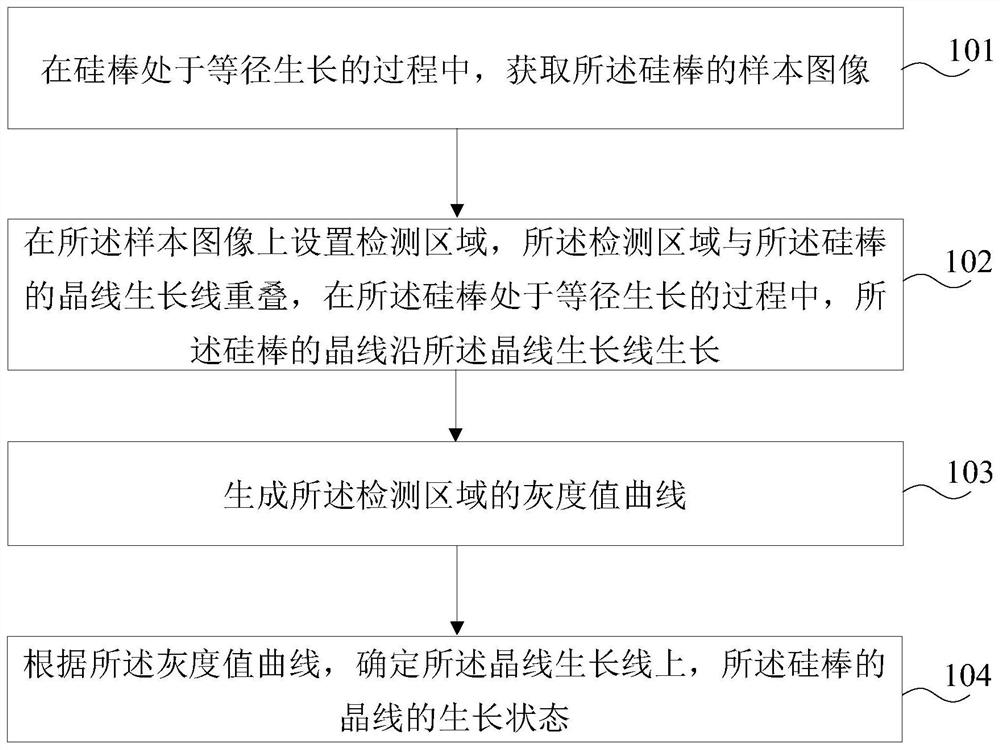
[0070] refer to figure 1 , figure 1 A flow chart of the steps of a method for detecting the growth state of a silicon rod crystal line in Embodiment 1 of the present invention is shown. The method may include the steps of:
[0071] Step 101 , acquiring a sample image of the silicon rod while the silicon rod is growing in equal diameter.
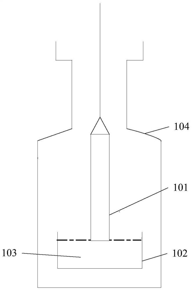
[0072] refer to figure 2 , shows a schematic diagram of a silicon rod preparation device in Embodiment 1 of the present invention.
[0073] In the embodiment of the present invention, when using the Czochralski method to prepare single crystal silicon, the single crystal furnace 104 is used to melt high-purity polycrystalline silicon material in the quartz crucible 102, and the lower end of the single crystal seed crystal is immersed in the quartz crucible The liquid surface of the molten silicon 103, and the lower end of the single crystal seed crystal are sequentially subjected to the seeding, shouldering, shoulder turning, equal-diame...
Embodiment 2
[0099] see Figure 5 , shows a flow chart of the steps of a method for detecting the state of crystal line growth of a silicon rod in Embodiment 2 of the present invention, and the method may include the following steps:
[0100] Step 201 , acquiring a sample image of the silicon rod when the silicon rod is growing in equal diameter.
[0101] For this step, reference may be made to the above-mentioned step 101 for details, which will not be repeated here.
[0102] Step 202: Perform image enhancement processing on the sample image according to a preset image enhancement algorithm.
[0103] In this step, image enhancement can be performed on the sample image of the silicon rod to enhance the characteristics of the crystal lines in the sample image, and expand the difference between the crystal lines and other regions in the sample image, which is beneficial to improve the follow-up according to the sample image. The gray value curve corresponding to the detection area determines...
Embodiment 3
[0175] refer to Figure 14 , which shows a structural block diagram of a silicon rod crystal line growth state detection device in Embodiment 3 of the present invention, which may specifically include:
[0176] The sample image acquisition module 301 is configured to acquire a sample image of the silicon rod when the silicon rod is growing in equal diameter.
PUM
 Abstract
Description
Claims
Application Information