Silicon wafer drying device and method

A technology for drying devices and silicon wafers, which is applied in the directions of drying gas arrangement, drying solid materials, and dry cargo handling, etc. It can solve problems such as increasing drying time, affecting process coating process, and affecting production capacity.

Pending Publication Date: 2021-03-09
SUZHOU SHENGCHENG SOLAR EQUIP
View PDF0 Cites 4 Cited by
  • Summary
  • Abstract
  • Description
  • Claims
  • Application Information

AI Technical Summary

Problems solved by technology

[0004] The drying process of the silicon wafer after cleaning is usually blown and dried with heated high-pressure air. At this time, the surface of the silicon wafer is in a hot and humid environment with sufficient oxygen. Oxidation, but high-efficiency batteries have high standards for the surface of the silicon wafer, the oxide layer on the surface of the silicon wafer should not be too thick, otherwise it will affect the subsequent process, especially the coating process, so in order to reduce the surface oxidation of the sil

Method used


Image

  • Silicon wafer drying device and method
  • Silicon wafer drying device and method

Examples


Embodiment Construction

[0022] The preferred embodiments of the present invention will be described in detail below in conjunction with the accompanying drawings, so that the advantages and features of the invention can be more easily understood by those skilled in the art, so as to define the protection scope of the present invention more clearly.

[0023] see figure 1 and figure 2 , the embodiment of the present invention includes:

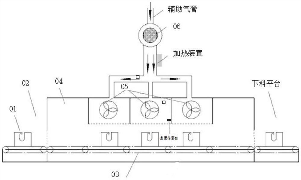
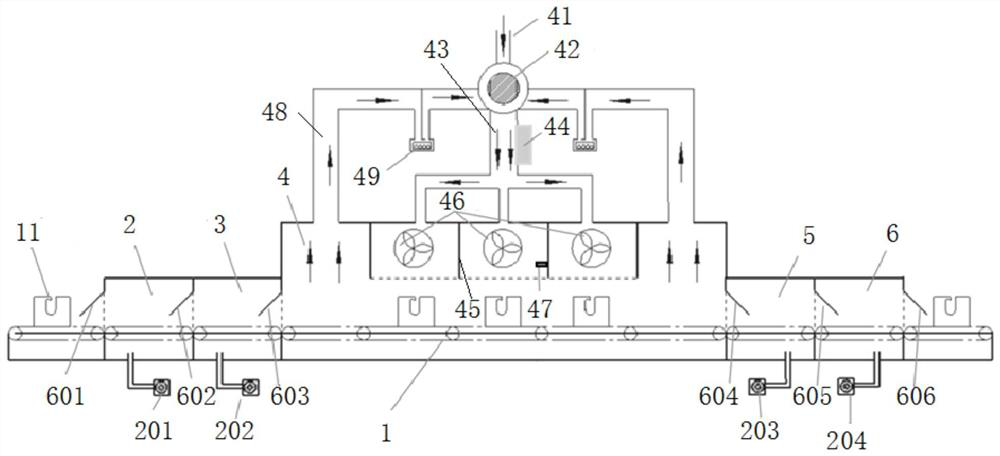
[0024] A silicon wafer drying device, the silicon wafer drying device comprises a texture basket transfer device 1, a first buffer chamber 2, a first low-pressure chamber 3, a drying chamber 4, a second low-pressure chamber 5, a second buffer chamber 6, a vacuum system, filtration and reduction system, heating temperature control system, gas purging system and water vapor condensation circulation system, the texturing flower basket conveying device 1 is used to transport the texturing flower baskets 11 loaded with silicon wafers arranged at equal distances, and the t...


PUM


Abstract

The invention discloses a silicon wafer drying device and method. The silicon wafer drying device comprises a texturing basket conveying device, a first buffering cavity, a first low-pressure cavity,a drying cavity, a second low-pressure cavity and a second buffering cavity; the texturing basket conveying device is used for conveying texturing baskets which load silicon wafers and are arranged atequal intervals, the texturing basket conveying device is sequentially provided with the first buffering cavity, the first low-pressure cavity, the drying cavity, the second low-pressure cavity and the second buffering cavity in the conveying direction, the cavities are separated into closed spaces through double side doors, the buffering cavities and the low-pressure cavities are connected witha vacuum system, and a gas filtering reduction system, a heating temperature control system, a gas purging system and a water vapor condensation circulating system are arranged in the drying cavity. By means of the above manner, the textured silicon wafers and the texturing baskets can be dried, silicon wafer surface oxidation caused by water vapor and oxidizing atmosphere in the drying process isavoided, and poor product manufacturing procedures are reduced.

Description

technical field [0001] The invention relates to the technical field of semiconductor device production, in particular to a silicon wafer drying device and a method thereof. Background technique [0002] Environmental pollution and energy crisis have become increasingly prominent. In recent years, my country has paid attention to the adjustment of energy structure, given priority to the development of clean energy, and achieved significant results. Solar energy is inexhaustible and inexhaustible. It is the new energy source with the most development potential. The main force of the future energy system, solar cells are devices that can convert solar energy into electrical energy. The technology is mainly divided into three categories: the first category is single crystal / polycrystalline traditional diffusion technology, which has low efficiency and has been eliminated by the market; the second category It is PERC technology, which is an upgrade of the previous technology. After...

Claims


Application Information

Patent Timeline
IPC IPC(8): F26B15/14F26B21/00F26B21/04F26B21/08F26B25/00F26B25/18
CPCF26B15/14F26B21/001F26B21/004F26B21/04F26B21/086F26B25/00F26B25/003F26B25/18
Inventor 杨星李长江周文彬
Owner SUZHOU SHENGCHENG SOLAR EQUIP
Why Eureka
Try Eureka