Heterojunction semiconductor device resistant to impact with avalanche

A semiconductor and heterojunction technology, applied in the direction of semiconductor devices, electrical components, circuits, etc., can solve the problems of easy burnout, lack of surge robustness, and inability to withstand surge current shocks. The effect of surge robustness

Active Publication Date: 2021-03-09
SOUTHEAST UNIV
View PDF2 Cites 0 Cited by
  • Summary
  • Abstract
  • Description
  • Claims
  • Application Information

AI Technical Summary

Problems solved by technology

[0004] However, traditional heterojunction semiconductor devices do not have avalanche capability, cannot withstand the impact of surge current, do not have surge robustness, and are easy to be burned. Therefore, traditional heterojunction semiconductor devices need to be improved. This patent That is, a heterojunction semiconductor device with avalanche resistance is designed, which improves the surge robustness of the device

Method used


Image

  • Heterojunction semiconductor device resistant to impact with avalanche
  • Heterojunction semiconductor device resistant to impact with avalanche
  • Heterojunction semiconductor device resistant to impact with avalanche

Examples


Embodiment Construction

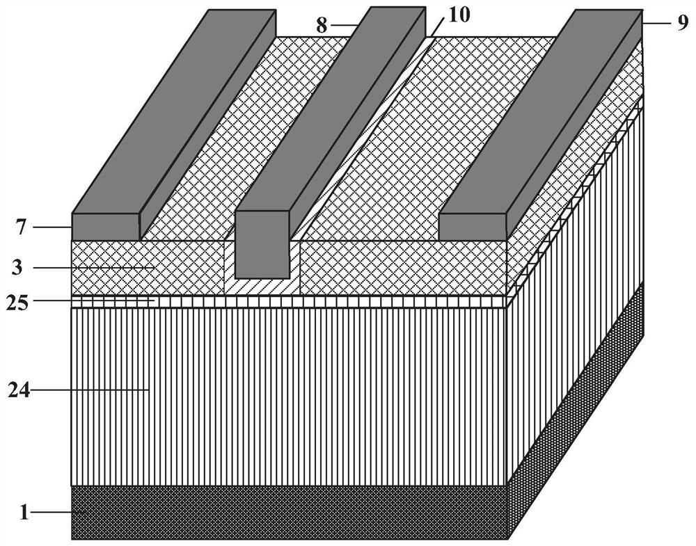
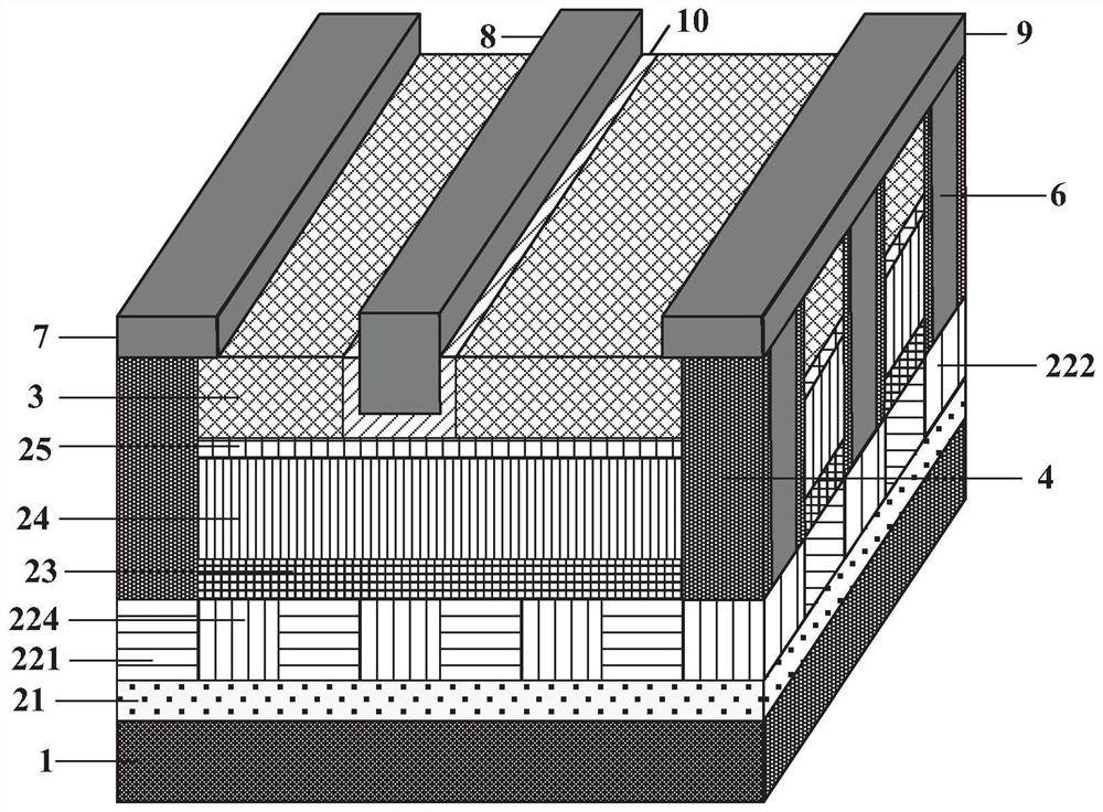
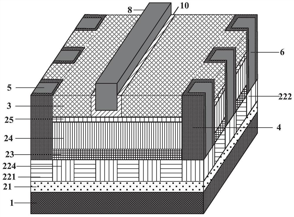
[0029] An avalanche-resistant heterojunction semiconductor device, comprising: a substrate 1 and a second dielectric layer 23, a first dielectric layer 21 is disposed on the substrate 1, and a first semiconductor semiconductor device is disposed on the second dielectric layer 23 Layer 24, the first semiconductor layer 24 is provided with the second semiconductor layer 3, the first semiconductor layer 24 is in contact with the second semiconductor layer 3 to form a conductive channel layer 25, and the second semiconductor layer 3 is provided with a metal source electrode 7, The metal gate electrode 8 and the metal drain electrode 9 are provided with a third dielectric layer 10 between the second semiconductor layer 3 and the metal gate electrode 8, and are characterized in that a dielectric layer 10 is provided between the first dielectric layer 21 and the second dielectric layer 23 There is an avalanche layer and the avalanche layer is connected to the metal source electrode 7 ...


PUM


Abstract

The invention discloses a heterojunction semiconductor device resistant to impact with avalanche, which comprises a substrate (1) and a second dielectric layer (23), wherein a first dielectric layer (21) is arranged on the substrate (1), a first semiconductor layer (24) is arranged on the second dielectric layer (23), a second semiconductor layer (3) is arranged on the first semiconductor layer (24), the first semiconductor layer (24) and the second semiconductor layer (3) are contacted to form a conductive channel layer (25), a metal source electrode (7), a metal gate electrode (8) and a metal drain electrode (9) are arranged on the second semiconductor layer (3), and a third dielectric layer (10) is arranged between the second semiconductor layer (3) and the metal gate electrode (8). Theheterojunction semiconductor device is characterized in that an avalanche layer is arranged between the first dielectric layer (21) and the second dielectric layer (23) and is connected with the metal source electrode (7) and the metal drain electrode (9). The device has avalanche capability and high surge robustness.

Description

technical field [0001] The invention mainly relates to the field of high-voltage power semiconductor devices, in particular, it is a heterojunction semiconductor device capable of resisting impact by avalanche. Background technique [0002] As the third-generation semiconductor, the wide-bandgap semiconductor has become a research hotspot in the field of semiconductors. Compared with the first-generation and second-generation semiconductors, the wide-bandgap semiconductor has a wide bandgap, high breakdown electric field strength, and electron saturation drift rate. High, good thermal conductivity, strong radiation resistance and other characteristics. Larger bandgap width and high breakdown electric field strength greatly increase the peak voltage that wide bandgap semiconductor devices can withstand; high electron saturation drift rate enables devices to withstand higher frequencies; high thermal conductivity and good thermal stability The device can withstand a higher te...

Claims


Application Information

Patent Timeline
Patent Type & Authority Applications(China)
IPC IPC(8): H01L29/06H01L29/778
CPCH01L29/0619H01L29/7786
Inventor 刘斯扬辛树轩葛晨李胜张弛钱乐孙伟锋时龙兴
Owner SOUTHEAST UNIV
Why Eureka
Try Eureka