High frequency module and communication device
一种高频模块、高频信号的技术,应用在非印制电元件相联接的印刷电路、涂加非金属保护层、传输系统等方向,能够解决配置自由度限制、高频传输特性劣化、大空间等问题,达到提高设计自由度的效果
- Summary
- Abstract
- Description
- Claims
- Application Information
AI Technical Summary
Problems solved by technology
Method used
Image

Examples
Embodiment approach 1
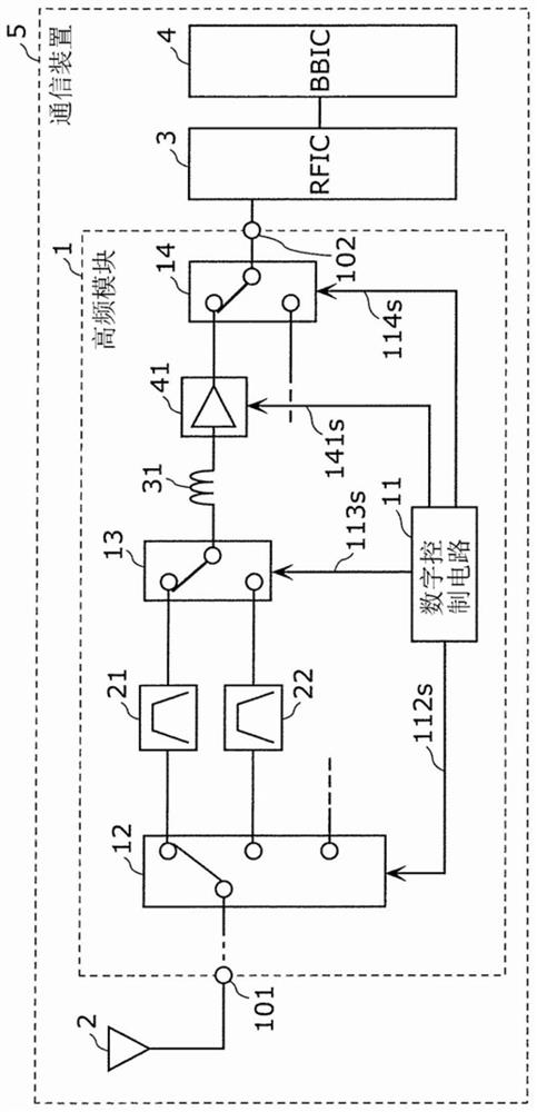
[0022] [1.1 Circuit structure of communication device and high-frequency module]
[0023] figure 1 It is a circuit block configuration diagram showing an example of the circuit configuration of the communication device 5 according to the first embodiment. As shown in the figure, the communication device 5 includes a high-frequency module 1 , an antenna element 2 , an RF integrated circuit (RFIC) 3 , and a baseband integrated circuit (BBIC) 4 . The high-frequency module 1 is arranged, for example, at the front end of a multi-mode / multi-band mobile phone.
[0024] The RFIC 3 is an RF signal processing circuit that processes high-frequency signals transmitted and received through the antenna element 2 . Specifically, RFIC3 performs signal processing on the high-frequency signal input via output terminal 102 of high-frequency module 1 by down-conversion or the like, and outputs a reception signal generated by the signal processing to BBIC4.
[0025] The BBIC 4 is a circuit that...
Embodiment approach 2
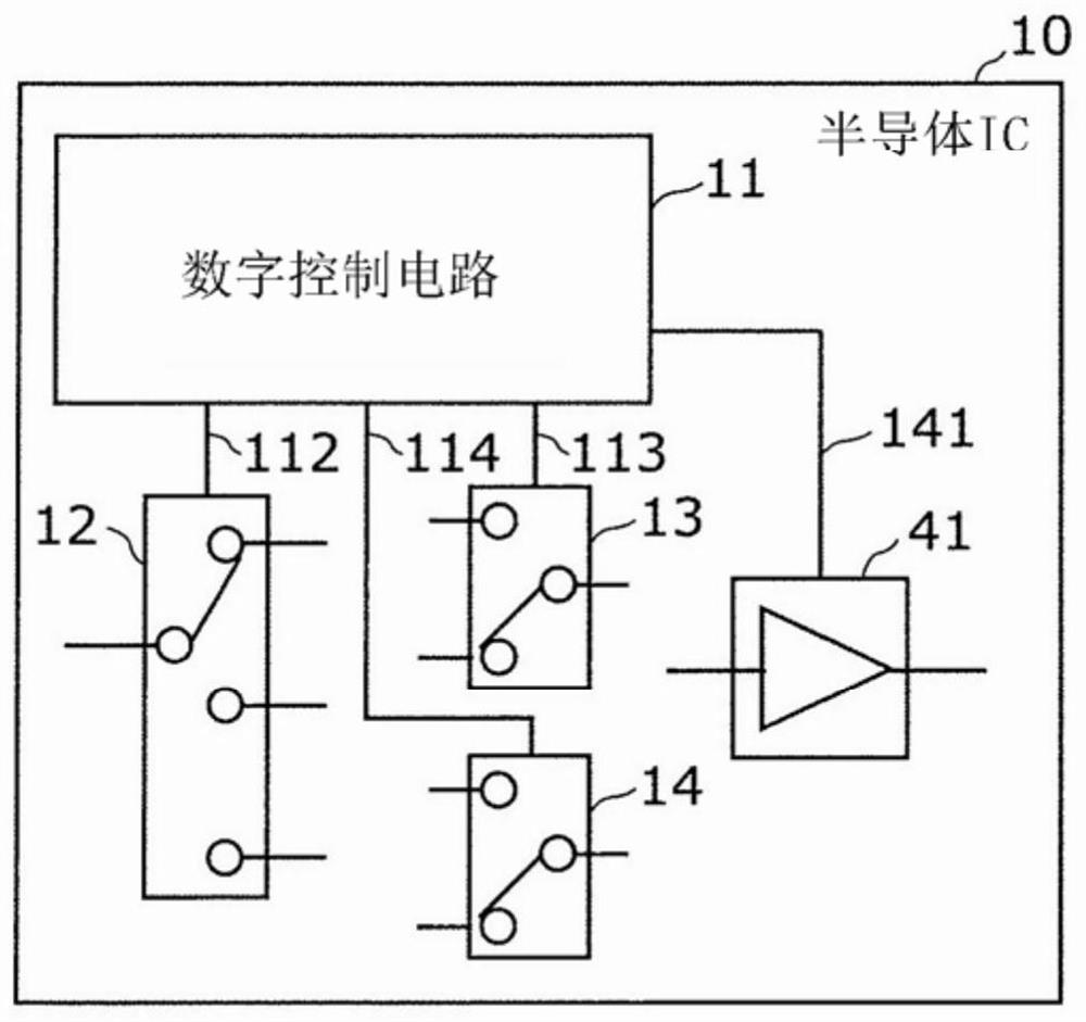
[0078] In this embodiment, an arrangement structure of an amplifier circuit built in the semiconductor IC 10 and matching circuit elements connected to the amplifier circuit will be described.
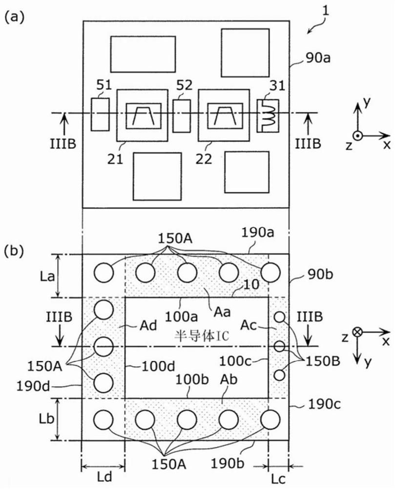
[0079] Figure 5A It is a schematic sectional structure diagram of the high frequency module 1B of Embodiment 2. In addition, regarding the planar structure of the high-frequency module 1B of this embodiment, the same as Figure 3A same. in particular, Figure 5A yes Figure 3A Sectional view on line IIIB-IIIB of .
[0080] Such as Figure 5A As shown, the high-frequency module 1B of this embodiment includes a module substrate 90, a semiconductor IC 10, a plurality of columnar electrodes 150A and 150B, filters 21 and 22, an inductor 31, circuit elements 51 and 52, and resin components 80A and 80B. . The high-frequency module 1B shown in the figure differs from the high-frequency module 1 according to Embodiment 1 in the point of showing the element arrangement structure in the s...
Embodiment approach 3
[0102] In this embodiment, the structure of the high frequency module which has the 3rd connection electrode extended from the main surface of semiconductor IC10 in the perpendicular direction of this main surface is demonstrated.
[0103] Figure 6 It is a schematic diagram which shows the planar structure and cross-sectional structure of the high frequency module 1C of Embodiment 3. exist Figure 6 (a) is a layout diagram of circuit elements when the main surface 90b of the main surfaces 90a and 90b of the module substrate 90 is viewed from the z-axis negative direction side. in addition, Figure 6 (b) is Figure 6 Sectional view on line VI-VI of (a). In addition, since the arrangement diagram of the circuit elements when the main surface 90a is viewed from the z-axis positive direction side is different from the Figure 3A (a) is the same, so the illustration is omitted.
[0104] Such as Figure 6 As shown, the high-frequency module 1C of this embodiment includes: a ...
PUM
 Abstract
Description
Claims
Application Information
 - R&D
- Intellectual Property
- Life Sciences
- Materials
- Tech Scout
- Unparalleled Data Quality
- Higher Quality Content
- 60% Fewer Hallucinations
Browse by: Latest US Patents, China's latest patents, Technical Efficacy Thesaurus, Application Domain, Technology Topic, Popular Technical Reports.
© 2025 PatSnap. All rights reserved.Legal|Privacy policy|Modern Slavery Act Transparency Statement|Sitemap|About US| Contact US: help@patsnap.com