Coherent near-field detection system based on free electron excitation and photoelectric detection

A technology of electron excitation and photoelectric detection, which is applied in the cross field of vacuum electronics and terahertz photodetection technology, can solve the contradiction between near-field coupling efficiency and imaging resolution, and can not directly see the spatial phase and resolution of the surface near-field depends on other issues

Active Publication Date: 2021-03-12
UNIV OF ELECTRONICS SCI & TECH OF CHINA
View PDF4 Cites 0 Cited by
  • Summary
  • Abstract
  • Description
  • Claims
  • Application Information

AI Technical Summary

Problems solved by technology

However, this type of near-field system has certain defects in detecting the near-field on the surface of materials or structures. For example, both excitation and detection come from the probe, so the spatial phase of the surface near-field cannot be directly seen; and the resolution of the system depends on the probe. , not only is it difficult to further improve, but also there is a contradiction between near-field coupling efficiency and imaging resolution

Method used


Image

  • Coherent near-field detection system based on free electron excitation and photoelectric detection
  • Coherent near-field detection system based on free electron excitation and photoelectric detection

Examples


Embodiment 1

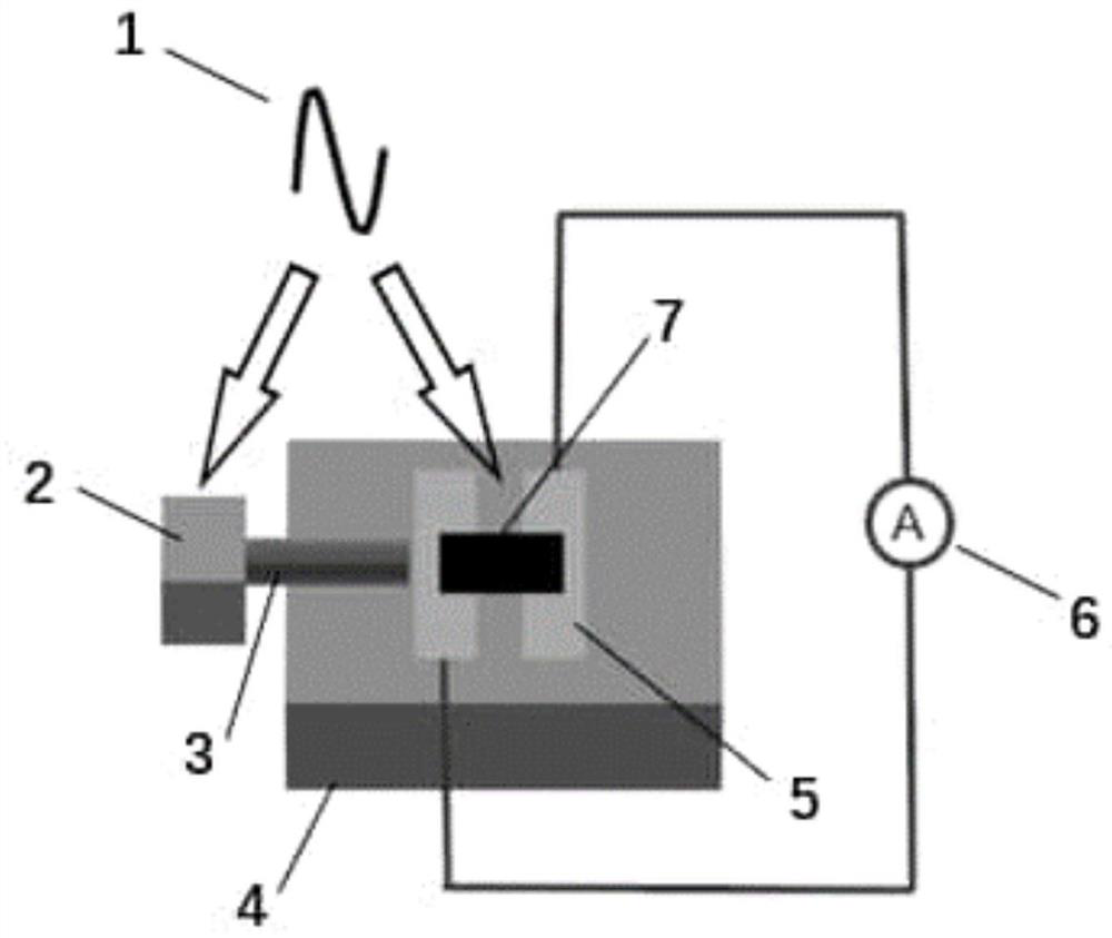
[0025] This example figure 1 As shown in , the femtosecond laser source produces a femtosecond laser with a certain repetition rate (such as 10MHz), and the femtosecond laser is divided into two beams by a beam splitter, which are used to excite the photocathode to generate photoelectron emission and excite the low temperature of the photoconductive antenna respectively. Gallium arsenide substrates generate freely moving charge carriers. Among them, the femtosecond laser connected to the photoconductive antenna needs to pass through an optical delay optical path (not shown in the figure), and then converge from the lower surface of the photoconductive antenna to the slit of the two metal electrodes. The corresponding 2D material to be tested. The pulsed electron beam generated by the photocathode skims the surface of the photoconductive antenna. When the electron projected field passes between the two metal electrodes of the photoconductive antenna, corresponding surface wave...

Embodiment 2

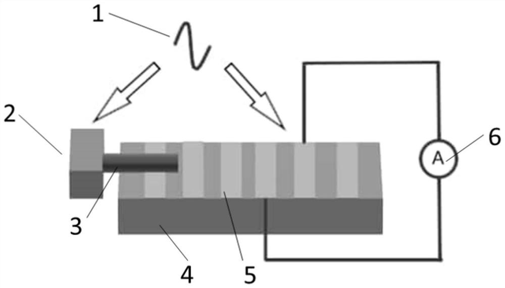
[0027] This example figure 2 As shown, the principle is similar to the first embodiment, except that the material to be tested is a metal grating structure, so two adjacent metal gratings are used as metal electrodes. The surface wave of the metal grating structure is generated by the interaction between the pulsed electron beam and the metal grating. Two adjacent metal gratings are used as the electrodes of the photoconductive antenna. The substrate is also made of low-temperature gallium arsenide. The propagation of the surface wave leads to a gap between the metal gratings used as electrodes. A changing potential difference is produced. This method can detect surface waves with different frequencies caused by changing the grating parameters.


PUM


Abstract

The invention discloses a coherent near-field detection system based on free electron excitation and photoelectric detection, and belongs to the crossing field of vacuum electronics and terahertz photoelectric detection technologies. A femtosecond laser source is adopted to generate femtosecond laser, the femtosecond laser is divided into two beams by a beam splitter, one beam excites a photocathode to generate a pulsed electron beam, the pulsed electron beam excites a surface wave of a to-be-measured material, and a photoconductive antenna composed of a substrate and a metal electrode is placed on the lower surface of the to-be-measured material (if the to-be-measured material is a metal grating; if not, two adjacent gratings are used as metal electrodes) to directly sense the surface wave of the to-be-measured material; and the other beam of femtosecond laser is injected into the photoconductive antenna through the time-delay light path, so that photoelectric sampling is realized, and the detection of the surface wave of the to-be-measured material is completed. According to the method, the influence of the needle tip on the near-field signal is avoided, the intensity of the electron projection field on the surface of the object is far less than that of the surface wave, and the time domain direct detection of the relatively pure near-field signal can be realized.

Description

technical field [0001] The invention belongs to the intersecting field of vacuum electronics and terahertz photoelectric detection technology, and relates to a photocathode photoelectron emission and a time-domain detection method of a photoconductive antenna. Background technique [0002] Photocathode electron emission, together with thermal electron emission, field electron emission, and secondary electron emission, constitutes four basic forms of electron emission; in the process of photocathode electron emission, the electrons inside the cathode material absorb the laser photon energy , produce an energy level transition and leave the surface of the material, and finally complete electron emission, and the emission period is consistent with the pulse laser repetition period. [0003] Photoconductive antennas are terahertz generation or detection devices based on semiconductors (commonly used materials are gallium arsenide and sapphire silicon wafers) and bimetallic anten...

Claims


Application Information

Patent Timeline
Patent Type & Authority Applications(China)
IPC IPC(8): G01N21/62G01R29/08
CPCG01N21/62G01R29/0885G01N2021/625
Inventor 胡旻许星星张倬铖张晓秋艳张天宇王月莹常少杰肖丰钟任斌吴振华刘盛纲
Owner UNIV OF ELECTRONICS SCI & TECH OF CHINA
Why Eureka
Try Eureka