Deep ultraviolet light emitting diode and manufacturing method thereof

A technology of light-emitting diodes and manufacturing methods, which is applied to semiconductor devices, electrical components, circuits, etc., and can solve problems such as high defect density, large gaps, and low internal quantum efficiency

Active Publication Date: 2021-03-16
HANGZHOU SILAN AZURE +1
View PDF7 Cites 5 Cited by
  • Summary
  • Abstract
  • Description
  • Claims
  • Application Information

AI Technical Summary

Problems solved by technology

At present, the quantum efficiency of deep ultraviolet LED products is very low, generally no more than 10%, and there is a big gap compared with blue-green LED products. The quantum efficiency is low; secondly, P-GaN is used as the ohmic contact, and there is a serious phenomenon of deep ultraviolet light absorption; thirdly, with the increase of the Al composition in the quantum well, the light emitted by the deep ultraviolet LED is in the TM-Transverse Magnetic transverse magnetic mode (parallel Based on the light-emitting surface), it is difficult for TM light to enter the escape cone of the light-emitting surface and exit the LED device. The light extraction efficiency of TM is only one tenth of the light extraction efficiency of TE-Transverse electrical mode
These problems seriously restrict the performance improvement of deep ultraviolet LED chips

Method used


Image

  • Deep ultraviolet light emitting diode and manufacturing method thereof
  • Deep ultraviolet light emitting diode and manufacturing method thereof
  • Deep ultraviolet light emitting diode and manufacturing method thereof

Examples


Embodiment Construction

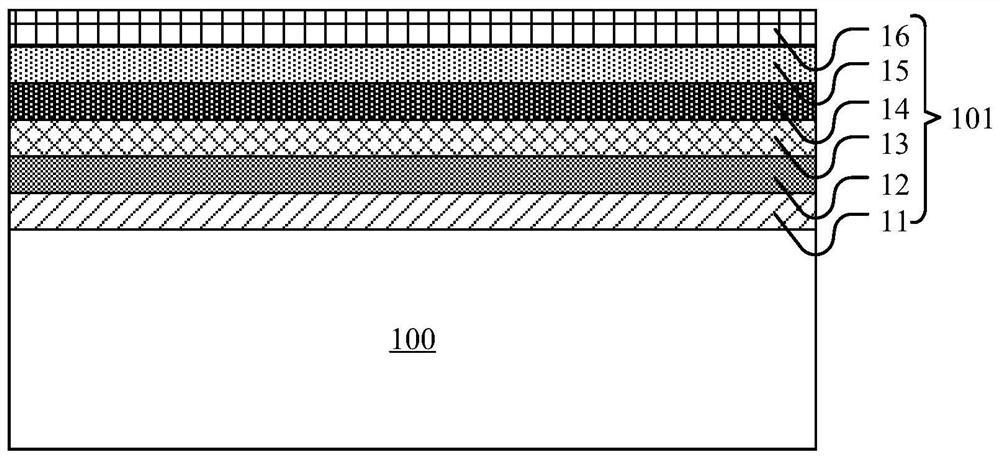
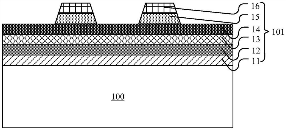
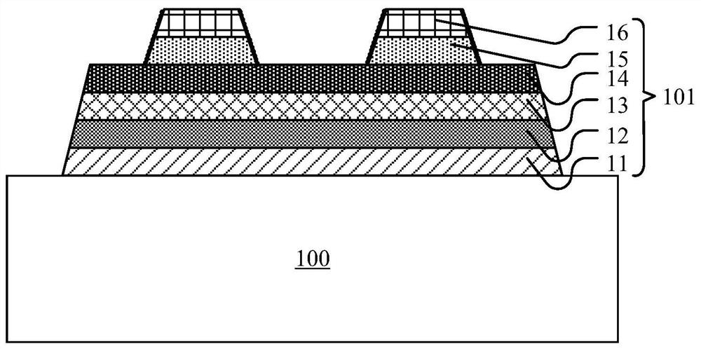
[0072] Hereinafter, the present invention will be described in more detail with reference to the accompanying drawings. In the various figures, identical elements are indicated with similar reference numerals. For the sake of clarity, various parts in the drawings have not been drawn to scale. Also, some well-known parts may not be shown. For the sake of simplicity, the semiconductor structure obtained after several steps can be described in one figure.

[0073] It should be understood that when describing the structure of a device, when a layer or a region is referred to as being "on" or "over" another layer or another region, it may mean being directly on another layer or another region, or Other layers or regions are also included between it and another layer or another region. Also, if the device is turned over, the layer, one region, will be "below" or "beneath" the other layer, or region.

[0074] If it is to describe the situation directly on another layer or anothe...


PUM

PropertyMeasurementUnit
thicknessaaaaaaaaaa
thicknessaaaaaaaaaa
thicknessaaaaaaaaaa

Abstract

The invention discloses a deep ultraviolet light emitting diode and a manufacturing method thereof. The deep ultraviolet light emitting diode comprises an epitaxial layer, a first ohmic contact layerand a second ohmic contact layer; the epitaxial layer comprises a first semiconductor layer, a multi-quantum well layer and a second semiconductor layer, the epitaxial layer comprises a first step, the step surface of the first step is the surface of the second semiconductor layer, the side wall of the first step is the side wall of the multi-quantum well layer and the side wall of the second semiconductor layer, and the other step surface of the first step is the surface of the first semiconductor layer; the first ohmic contact layer is in contact with the first semiconductor layer; and the second ohmic contact layer is in contact with the second semiconductor layer. According to the invention, the first steps in array distribution are formed in the epitaxial layer of the deep ultravioletlight emitting diode, and a roughened surface is formed on the side wall of each first step, so that the area ratio of the side wall of the deep ultraviolet light emitting diode is increased, and thelight extraction efficiency of the deep ultraviolet light emitting diode is improved.

Description

technical field [0001] The invention relates to the technical field of semiconductor chips, in particular to a deep ultraviolet light-emitting diode and a manufacturing method thereof. Background technique [0002] In recent years, the application of deep ultraviolet LED (light emitting diode) has shown explosive growth. Deep ultraviolet rays have a broad-spectrum bactericidal effect on various germs. Airborne pathogenic microorganisms such as influenza viruses (flu), rhinoviruses (common cold) and more dangerous pathogens (coronaviruses, etc.) are responsible for many diseases. Deep ultraviolet rays can not only directly kill bacteria on the surface of objects, but also penetrate air and water to kill bacteria in them, which has a very wide range of application scenarios. [0003] However, deep ultraviolet LED products still face serious problems, and related technologies still need to be significantly improved. At present, the quantum efficiency of deep ultraviolet LED ...

Claims


Application Information

Patent Timeline
Patent Type & Authority Applications(China)
IPC IPC(8): H01L33/18H01L33/14H01L33/24H01L33/44H01L33/46
CPCH01L33/18H01L33/14H01L33/24H01L33/44H01L33/46
Inventor 范伟宏薛脱李东昇张晓平马新刚高默然赵进超
Owner HANGZHOU SILAN AZURE
Why Eureka
Try Eureka