Organic light-emitting device, preparation method thereof and display device comprising organic light-emitting device
An electroluminescent device and electroluminescent technology, which are applied in the fields of electro-solid devices, semiconductor/solid-state device manufacturing, electrical components, etc., to achieve the effect of improving device efficiency and service life
- Summary
- Abstract
- Description
- Claims
- Application Information
AI Technical Summary
Problems solved by technology
Method used
Image
Examples
preparation example Construction
[0108] Preparation method of organic electroluminescence device
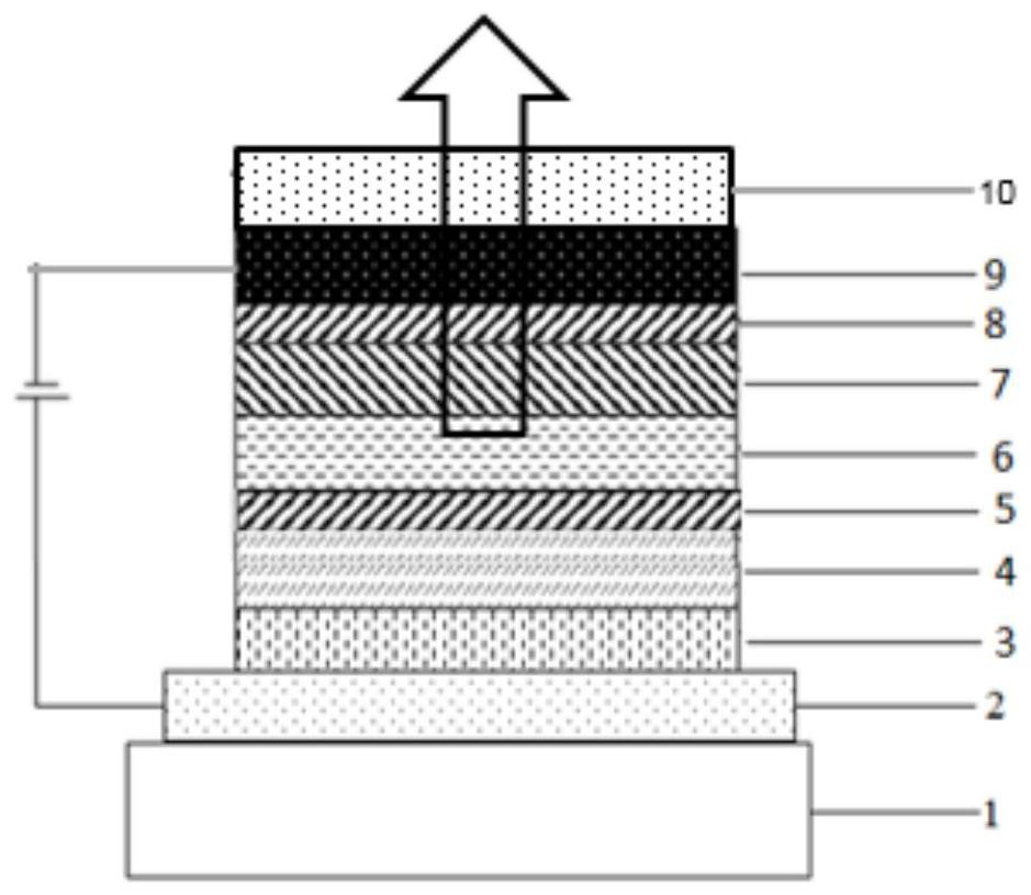
[0109] The present invention also relates to a method for preparing the above-mentioned organic electroluminescence device, which comprises sequentially laminating a first electrode, an organic functional material layer and a second electrode on a substrate. Wherein, the organic functional material layer is formed by sequentially laminating a hole transport region, a light-emitting layer and an electron transport region on the first electrode from bottom to top, and the hole transport region is successively layered on the first electrode from bottom to top A hole injection layer, a hole transport layer and an electron blocking layer are formed by pressing a hole injection layer, a hole transport layer and an electron blocking layer, and the electron transport region is formed by sequentially laminating a hole blocking / electron transport layer and an electron injection layer on the light emitting layer from bott...
Embodiment 1
[0174] Vacuum evaporation was carried out under the following conditions: using OLED ChusterDeposition System (manufacturer: CHOSHU INDUSTRY Co.LTD.) vacuum evaporation equipment model 1504-10117-01-0, at a vacuum degree of 1.0 × 10 -7 Torr pressure, wherein, when only one material is used to form a layer, the evaporation rate is controlled as If two or more materials are used in the same layer, each of the several materials used is placed in an evaporation source, and its evaporation rate is set separately so that the ratio of the evaporation rate is equal to its mass ratio, For example, when the first and second host materials and dopant materials are used in the light-emitting layer, the three materials are respectively placed in three evaporation sources, and when their mass ratio is 50:50:6, their evaporation is controlled The rate is and
[0175] a) Use a transparent PI film as the substrate layer 1, wash it, that is, wash it with a cleaning agent (SemiClean M-L20)...
Embodiment 2 to Embodiment 20
[0185] An organic electroluminescent device was prepared in the same manner as in Example 1, except that in step e), the compounds shown in Table 2 were used to form the light-emitting layers of Examples 2 to 20, wherein in the first, When the ratio of the second host compound and the dopant material is 70:30:6, the evaporation rate is controlled as and And when the ratio of the three is 30:70:6, the evaporation rate is controlled to be and The specific device structure is shown in Table 2.
PUM
| Property | Measurement | Unit |
|---|---|---|
| thickness | aaaaa | aaaaa |
| thickness | aaaaa | aaaaa |
| thickness | aaaaa | aaaaa |
Abstract
Description
Claims
Application Information


