Vertical double-diffused transistor and manufacturing method thereof

A vertical double-diffusion and transistor technology, applied in semiconductor/solid-state device manufacturing, semiconductor devices, electrical components, etc., can solve the problems of no advantage of on-resistance, large isolation resistance, etc.

Pending Publication Date: 2021-04-02
JOULWATT TECH INC LTD
View PDF6 Cites 1 Cited by
  • Summary
  • Abstract
  • Description
  • Claims
  • Application Information

AI Technical Summary

Problems solved by technology

[0007] In the manufacturing process of the VDMOS device 100, an isolation photolithography plate needs to be added for high-energy injection, and the drain of the VDMOS device, that is, the N-type buried layer 102, is drawn out. However, with the increase of the device withstand voltage specification, the N The thickness of the N-type epitaxial layer 103 will also increase accordingly, so it will be difficult to lead out the N-type buried layer 102 by high-energy implantation. At the same time, the increase in the thickness of the N-type epitaxial layer 103 will also lead to a larger isolation resistance, so that the molded device will have no on-resistance. The advantages

Method used


Image

  • Vertical double-diffused transistor and manufacturing method thereof
  • Vertical double-diffused transistor and manufacturing method thereof
  • Vertical double-diffused transistor and manufacturing method thereof

Examples


Embodiment Construction

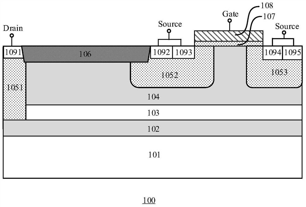
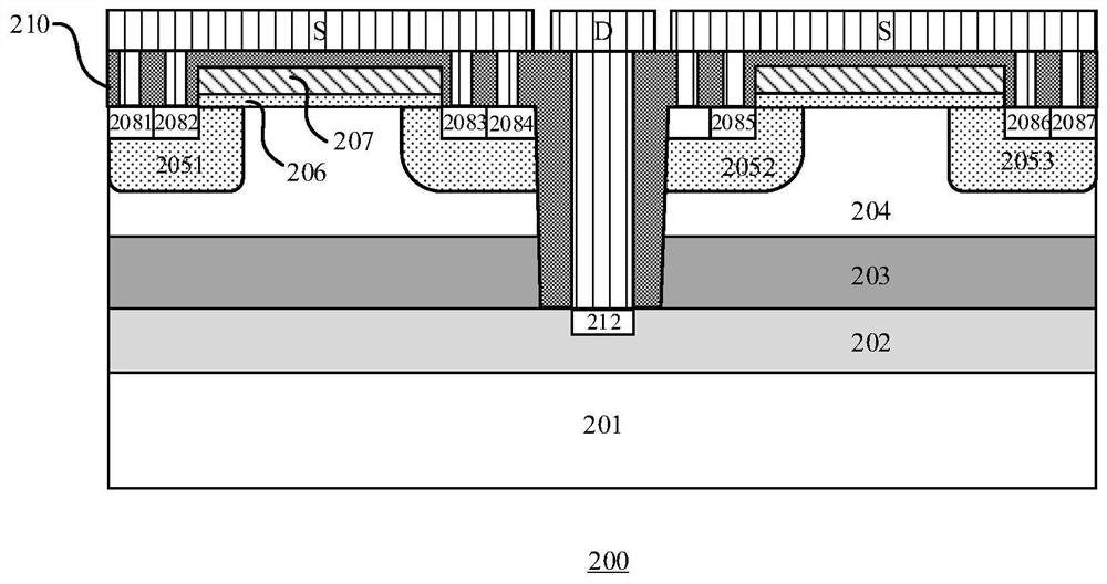
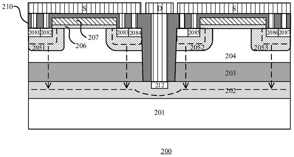
[0057] Various embodiments of the present disclosure will be described in more detail below with reference to the accompanying drawings. In the various drawings, the same elements are denoted by the same or similar reference numerals. For the sake of clarity, various parts in the drawings have not been drawn to scale. Also, some well-known parts may not be shown. For the sake of simplicity, the semiconductor structure obtained after several steps can be described in one figure.

[0058] Unless otherwise defined, all technical and scientific terms used in this disclosure have the same meaning as commonly understood by one of ordinary skill in the technical field to which this invention belongs. Terms used in the description of the present disclosure are for the purpose of describing specific embodiments only, and are not intended to limit the present disclosure. As used in this disclosure, the term "and / or" includes any and all combinations of one or more of the associated l...


PUM


Abstract

The invention relates to the technical field of semiconductors, and provides a vertical double-diffused transistor and a manufacturing method thereof. A formed VDMOS device is of an axial symmetry structure with the central axis of a first trench as the axis of symmetry; the VDMOS device forms metal contact in a drain region through the first trench penetrating to the upper surface of a first buried layer so as to lead out a drain electrode; and the led-out drain electrode is positioned on the top surface, far away from the substrate, of the high-voltage VDMOS device. Therefore, the VDMOS device can be integrated in a BCD process, driving capability with low on resistance and high current is realized, the drain electrode does not need to be led out from the bottom of a device structure, and the integration density of the device is improved. Meanwhile, at least two buried layer structures in longitudinal gradient distribution are used for replacing a drift region to form a PN junction with a body region, and the PN junction is close to a parallel plane junction by utilizing a drain electrode communicating to an injection region in the first buried layer when the device is reverselybroken down, so the withstand voltage of the VDMOS device is effectively improved.

Description

technical field [0001] The present disclosure relates to the technical field of semiconductors, in particular to a vertical double-diffusion transistor and a manufacturing method thereof. Background technique [0002] The BCD (Bipolar-CMOS-DMOS) process manufactures bipolar devices and CMOS devices on the same chip at the same time. It combines the advantages of high transconductance and strong load driving capability of bipolar devices with high integration and low power consumption of CMOS, so that they learn from each other and give full play to their respective advantages. The integrated BCD process of Bipolar / CMOS / DMOS is used to combine three different process types: bipolar is for analog control; CMOS is for digital control; DMOS is for processing high voltage and high current in chip or system management. Realize the soft start and power output of the system. Since the BCD process combines the respective advantages of the above three devices, BCD-based products can...

Claims


Application Information

Patent Timeline
Patent Type & Authority Applications(China)
IPC IPC(8): H01L29/78H01L29/06H01L21/336
CPCH01L29/7802H01L29/7803H01L29/0603H01L29/0615H01L29/0684H01L29/66712
Inventor 陈斌韩广涛
Owner JOULWATT TECH INC LTD
Why Eureka
Try Eureka