Semiconductor epitaxial structure, manufacturing method thereof and LED chip

A technology of epitaxial structure and manufacturing method, which is applied in the direction of semiconductor devices, electrical components, circuits, etc., to achieve the effects of improving crystal quality, reducing operating voltage, and increasing electron concentration

Pending Publication Date: 2021-04-09
XIAMEN CHANGELIGHT CO LTD
View PDF0 Cites 4 Cited by
  • Summary
  • Abstract
  • Description
  • Claims
  • Application Information

AI Technical Summary

Problems solved by technology

[0006] The purpose of the present invention is to provide a semiconductor epitaxial structure and it

Method used


Image

  • Semiconductor epitaxial structure, manufacturing method thereof and LED chip
  • Semiconductor epitaxial structure, manufacturing method thereof and LED chip
  • Semiconductor epitaxial structure, manufacturing method thereof and LED chip

Examples


Embodiment Construction

[0043] In order to make the content of the present invention clearer, the content of the present invention will be further described below in conjunction with the accompanying drawings. The invention is not limited to this specific example. Based on the embodiments of the present invention, all other embodiments obtained by persons of ordinary skill in the art without making creative efforts belong to the protection scope of the present invention.

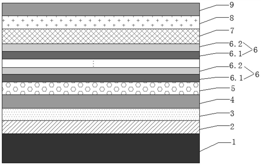
[0044] A semiconductor epitaxial structure, comprising:

[0045] substrate1;

[0046] The N-type semiconductor layer 4, the gate elimination layer 5, the active layer 7, and the P-type semiconductor layer 9 are sequentially stacked on the surface of the substrate 1; the gate elimination layer 5 includes an n-type doped semiconductor layer.

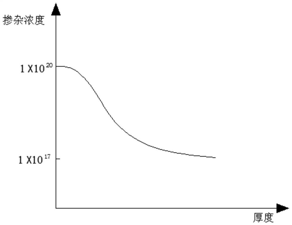
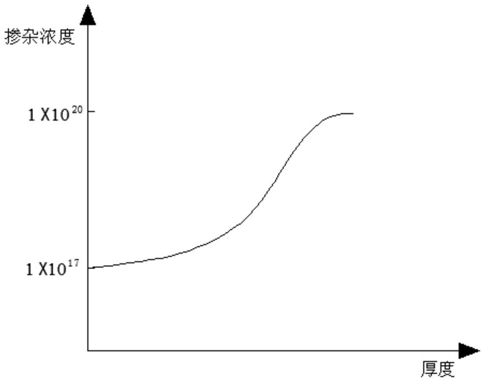
[0047] In the embodiment of the present invention, the gate elimination layer 5 includes a non-uniform n-type doped semiconductor layer.

[0048] It is worth mentioning that the type of the su...


PUM

PropertyMeasurementUnit
Thicknessaaaaaaaaaa

Abstract

The invention provides a semiconductor epitaxial structure, a manufacturing method thereof and an LED chip, and the method comprises the steps of sequentially stacking an N-type semiconductor layer, a gate elimination layer, an active layer and a P-type semiconductor layer on the surface of a substrate. Redundant electrons are released through the design of the epitaxial structure, the electron concentration is effectively improved, the electron tunneling probability is increased, the working voltage of an LED is reduced while the crystal quality is improved, and the anti-static capability of the LED is improved.

Description

technical field [0001] The invention relates to the field of light-emitting diodes, in particular to a semiconductor epitaxial structure, a manufacturing method thereof, and an LED chip. Background technique [0002] A light-emitting diode (English: Light Emitting Diode, referred to as: LED) is a semiconductor electronic component that can emit light. LED has the advantages of high efficiency, long life, small size, low power consumption, etc., and can be used in indoor and outdoor white light lighting, screen display, backlight and other fields. In the development of the LED industry, gallium nitride (GaN)-based materials are typical representatives of Group V-III compound semiconductors, and improving the photoelectric performance of GaN-based LEDs has become the key to the semiconductor lighting industry. [0003] Epitaxial wafers are the primary products in the LED manufacturing process. The existing GaN-based LED epitaxial wafer includes a substrate, an N-type semicon...

Claims


Application Information

Patent Timeline
IPC IPC(8): H01L33/14H01L33/00H01L33/36
CPCH01L33/14H01L33/005H01L33/36
Inventor 林志伟陈凯轩蔡建九卓祥景尧刚
Owner XIAMEN CHANGELIGHT CO LTD
Why Eureka
Try Eureka